Overview
The nRF51822 is a multi-protocol system-on-chip designed for ultra-low-power 2.4 GHz wireless applications, including Bluetooth low energy. It integrates a 32-bit ARM Cortex-M0 CPU with 256 KB flash and 16 KB RAM and a 2.4 GHz transceiver. The 2.4 GHz mode is wireless-compatible with the Nordic nRF24L series.
The device includes a range of analog and digital peripherals and supports interaction through the programmable peripheral interconnect (PPI) without CPU involvement. A flexible 31-pin GPIO mapping lets I/O functions such as serial interfaces, PWM, and demodulators be mapped to any package pin to maximize PCB design flexibility.
nRF51822 supports the S110 Bluetooth low energy protocol stack and a 2.4 GHz protocol stack (including Gazell); both stacks are available within the Nordic software development kit. Powering options include an internal linear regulator for supplies from 1.8 V to 3.6 V, and a DC-DC converter for supplies from 2.1 V to 3.6 V. Using the DC-DC converter can be controlled dynamically during operation and can reduce RF peak current to below 10 mA @ 3 V supply (TX @ 0 dBm & RX).
Available packages: 6 x 6 mm 48-pin QFN and a 3.5 x 3.8 mm 64-ball WLCSP.
Key Features
- Single-chip, multi-protocol 2.4 GHz device
- 32-bit ARM Cortex-M0 CPU core
- 256 KB flash, 16 KB RAM
- Support for S110 Bluetooth low energy stack (requires ~80 KB RAM)
- Thread safety and runtime protection
- Event-driven API
- Wireless compatibility with nRF24L series
- Three data rates: 2 Mbps / 1 Mbps / 250 kbps
- Up to +4 dBm output power
- -92.5 dBm sensitivity for Bluetooth low energy
- PPI system to minimize power consumption and simplify firmware
- Flexible power management with per-peripheral automatic control
- Configurable I/O mapping for analog and digital I/O
Smart Wristband Function and Connectivity
A smart wristband is a wearable device that records activity, sleep, and other lifestyle data. Data can be synchronized with phones, tablets, or PC clients over Bluetooth low energy 4.0 to enable health and activity tracking.
Typical features include setting user data (height, weight, stride), uploading activity records, and basic social sharing features via paired mobile clients. The wristband integrates a low-power Bluetooth 4.0 module to connect with phones, tablets, and PCs.
Hardware System Design
The wristband hardware circuit centers on the nRF51822 MCU and a set of MCU-controlled peripherals:
- Bluetooth RF circuitry
- SPI-connected G-sensor (accelerometer)
- I2C-controlled linear motor driver
- I2C-driven LED matrix driver, sharing the bus with the motor driver
- Button inputs via GPIO
- Status LEDs via GPIO
- Standard motor driver via GPIO with MOSFET
- External reset circuit
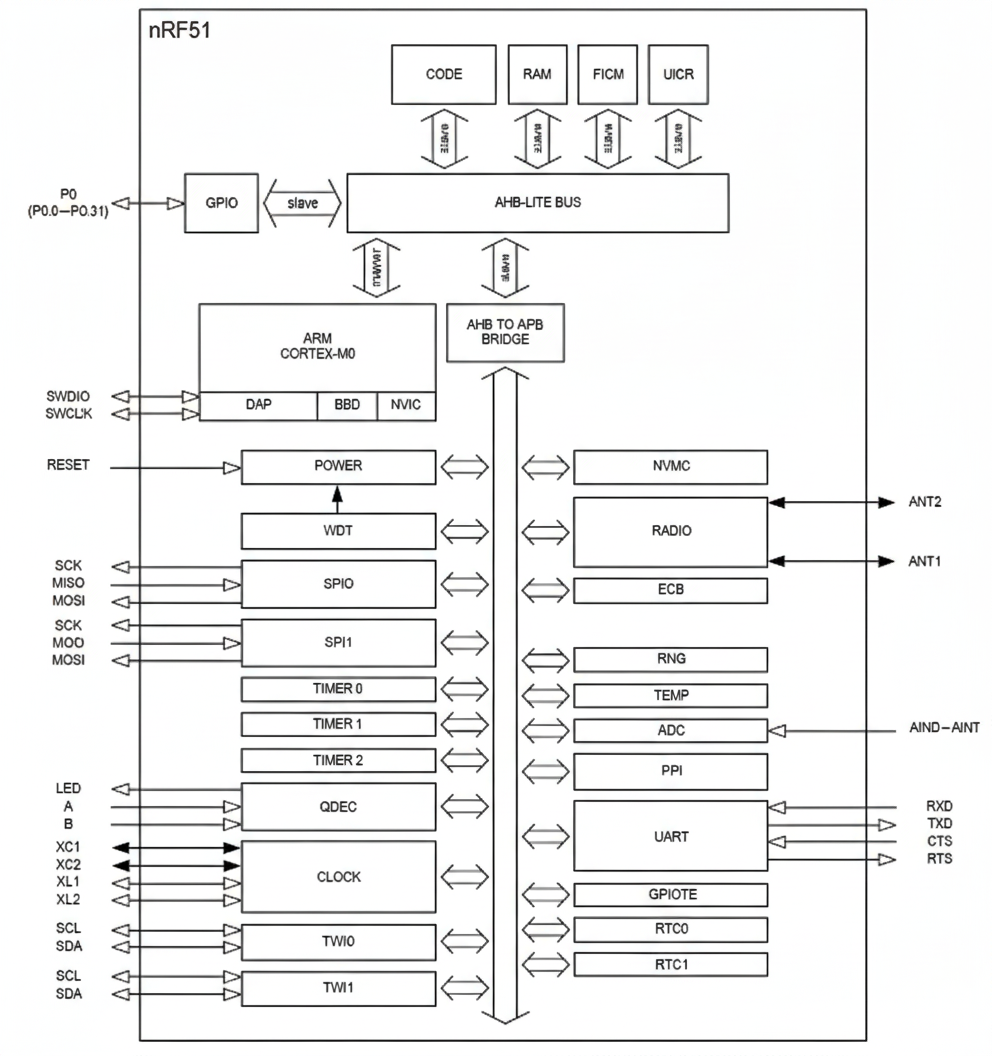
Figure 1: nRF51822 block diagram
Module Descriptions
1. MCU
The nRF51822 is the multi-protocol single-chip solution used for ultra-low-power wireless applications. It supports BLE 4.0 and 2.4 GHz protocol stacks and integrates the RF front end, an ARM Cortex-M0 core, 256 KB flash, and 16 KB RAM.
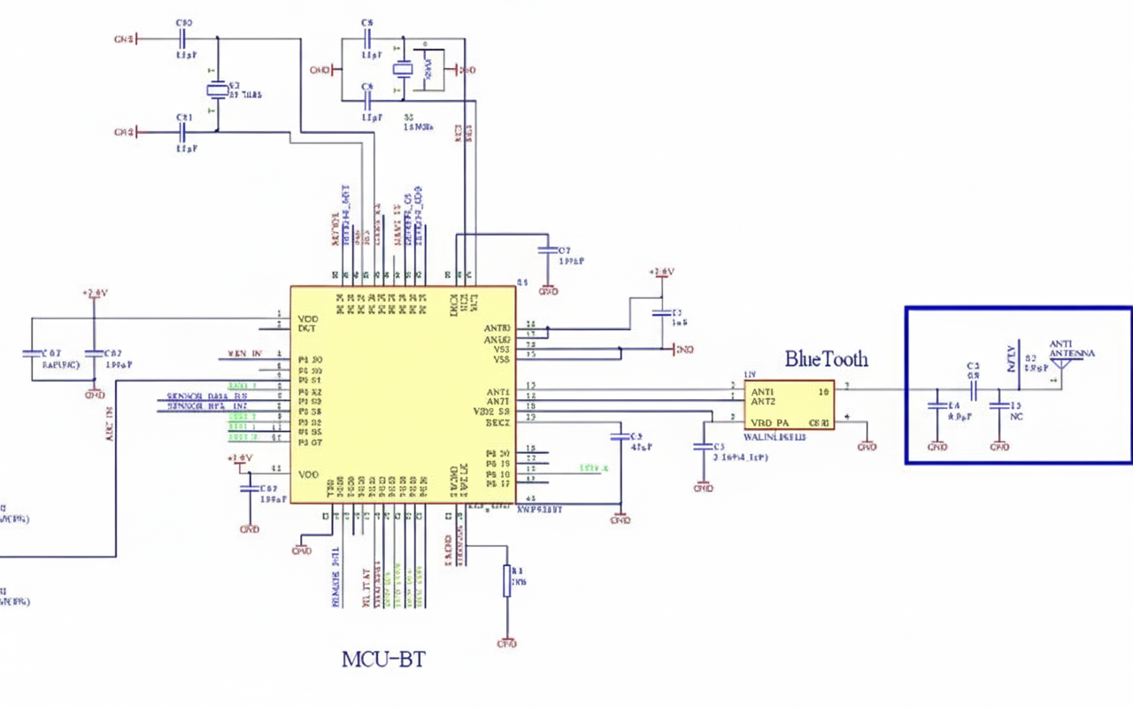
Figure 2: Wristband MCU circuit
2. G-sensor (Accelerometer)
The G-sensor senses acceleration changes from motion events like shaking, falling, ascending, or descending. The sensor converts acceleration forces to electrical signals, which the MCU analyzes to implement features such as step counting or gesture-based controls.
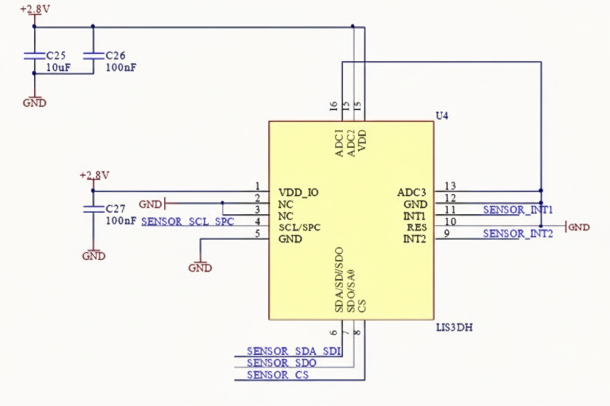
Figure 3: G-sensor circuit
3. Button Input Module
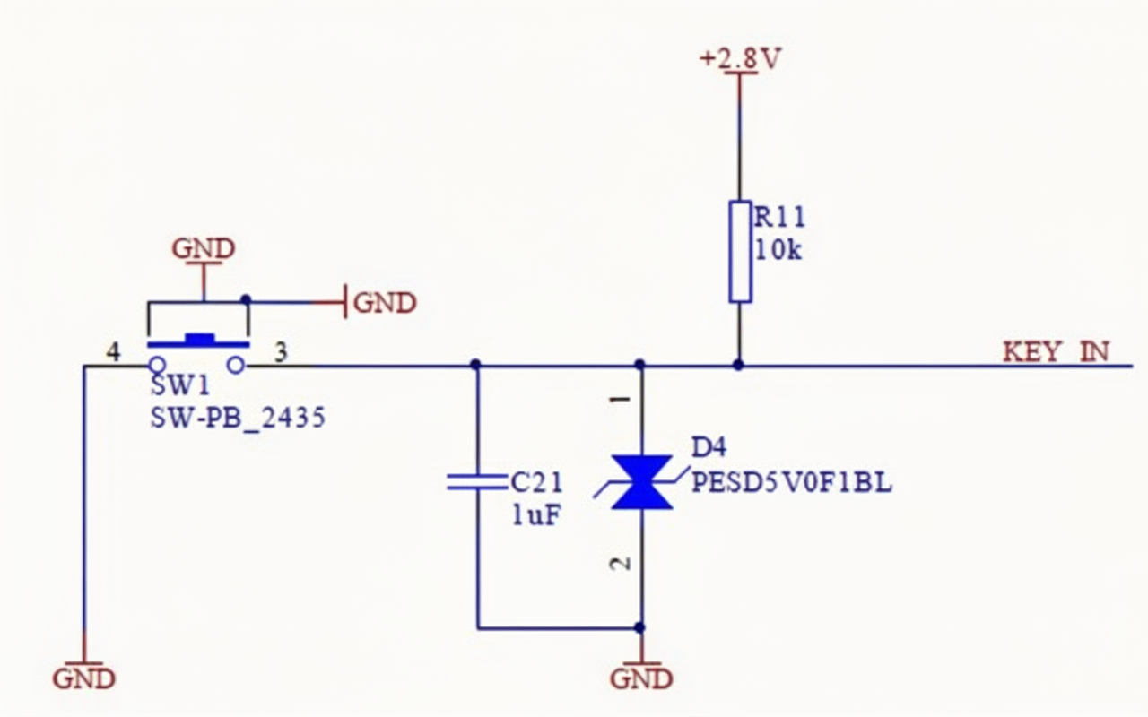
Figure 4: Button input module
4. LED Display
The LED display provides human interaction and data presentation. Two design options are typical:
- Multiple LED indicator approach for simple status display.
- LED dot-matrix display to present time, step count, calories, etc.
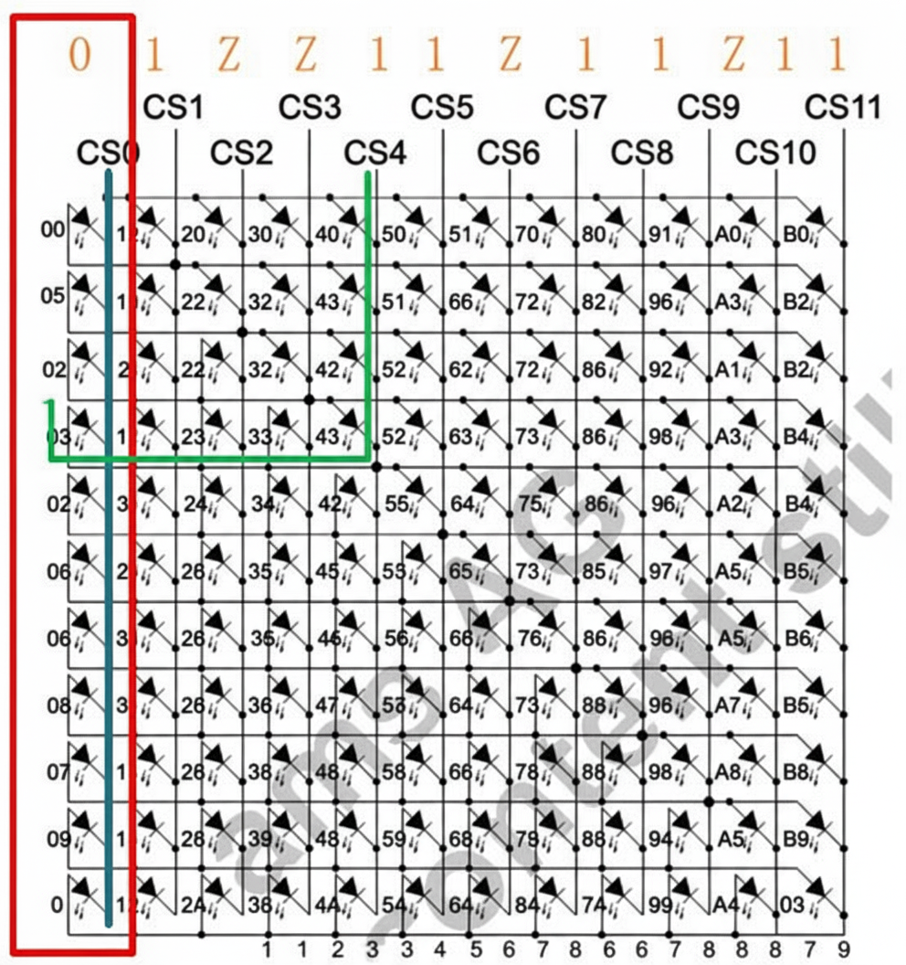
Figure 5: LED dot-matrix control module
5. Standard Motor Module
Standard vibration motors can draw up to 100 mA and cannot be driven directly from a GPIO. A MOSFET is used as a power-stage switch. A 24 Ω series resistor is used to adjust vibration intensity and reduce power consumption. With zero ohm, the motor startup current is approximately 100 mA; measured runtime current in the current configuration is about 36 mA.
A pull-down resistor on the MOSFET gate prevents the motor from briefly activating during system reset, because MCU pins can power up high momentarily.
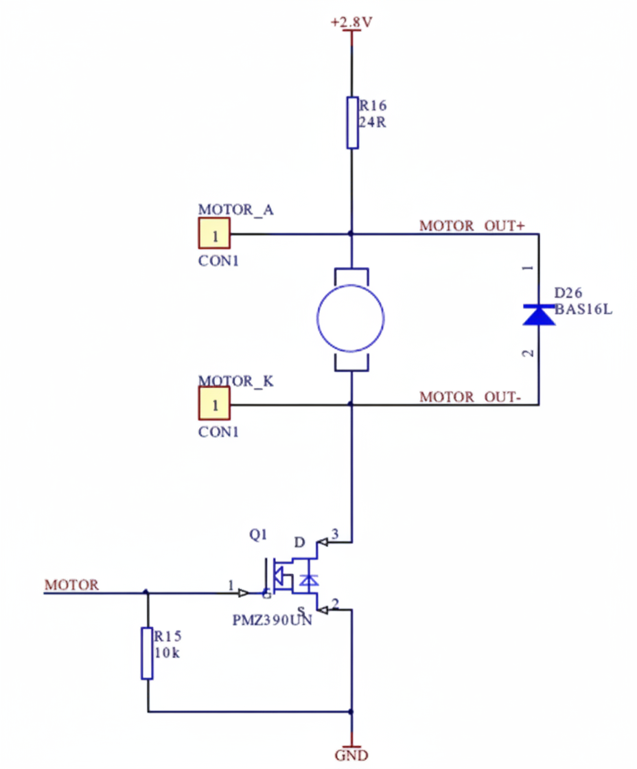
Figure 6: Standard motor module control circuit
6. Linear Motor Control Module
Linear motor control requires a dedicated driver IC. The design uses the DRV2605 driver, which communicates with the MCU over I2C. The driver controls motor functionality and accepts an input voltage range of 2.5 V to 5.5 V.
In this design, the driver is powered directly from the battery rather than the system DCDC output. This avoids double conversion losses: if both the system and the driver use DC-DC conversions, the effective efficiency may be reduced (for example, 90% x 90% = 81%).
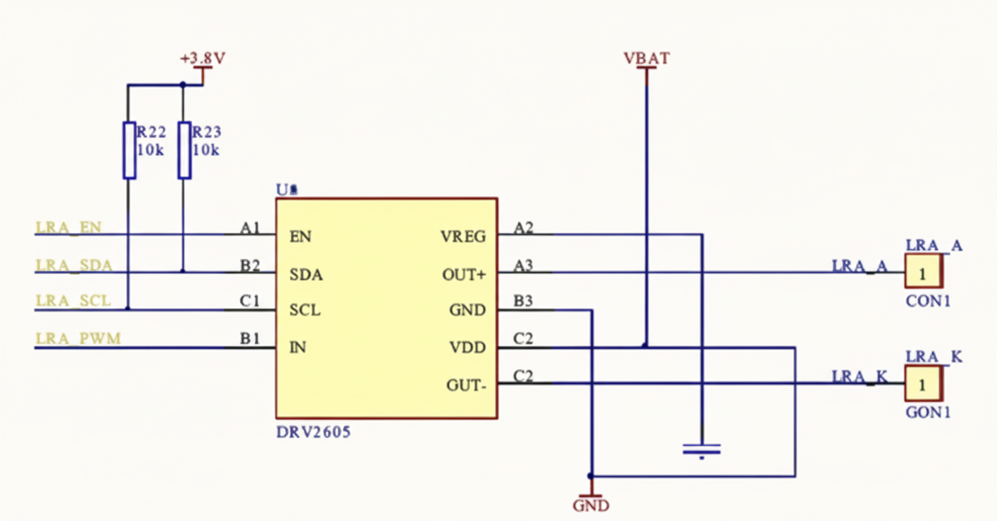
Figure 7: Linear motor control circuit
7. Battery Voltage Measurement
Battery remaining capacity is inferred from battery voltage. The design uses a quarter-voltage divider so that a battery voltage range of 0–4.2 V maps to 0–1.05 V, which fits within the nRF51822 ADC range of 0–1.2 V. A parallel resistor helps stabilize the measured voltage.
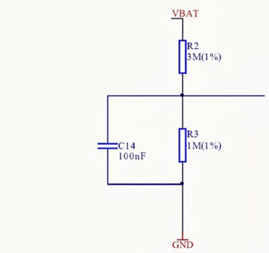
Figure 8: Battery voltage detection circuit
8. External Reset Module
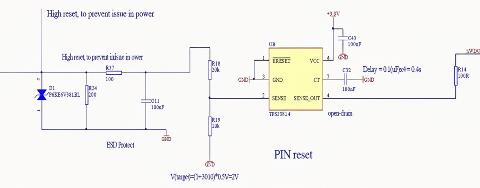
Figure 9: External reset circuit
9. Charging Circuit
The charging IC used is TI BQ24040. This part provides signals to the MCU indicating charging state (CHG_STATE) and whether a charger is connected (PG_STATE). Charging current and precharge/fast-charge ratios are configurable.
The reference design targets an 18 mAh battery, with a precharge current set to 40% of the fast charge current.
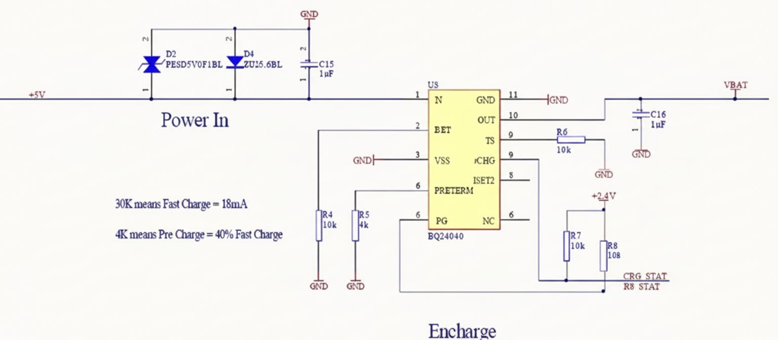
Figure 10: Charging circuit module
10. System Power Module
To maximize power efficiency, the design uses a high-efficiency, light-load-optimized DC-DC converter TPS62260 instead of a traditional LDO. Although LDOs have lower quiescent current, efficiency drops as VIN-VOUT increases. For example, with battery at 3.9 V and VOUT at 2.8 V, LDO efficiency is 2.8/3.9 = 71%.
DC-DC converters tend to have higher standby current, but once load current exceeds roughly 1 mA, overall efficiency can exceed 90%.
11. Debug Interface
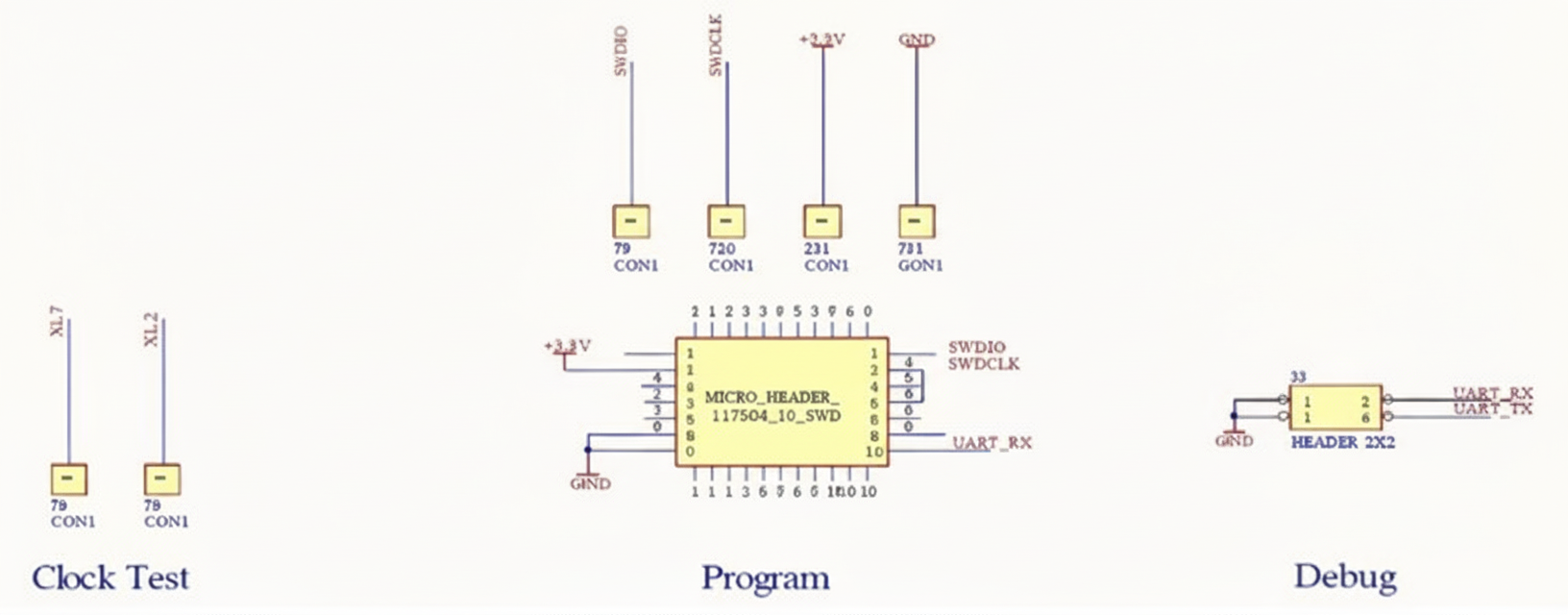
Figure 11: Debug interface
12. RF Layout Guidelines
- Place RF components close together and minimize trace length (1 mm of trace approximates 1 nH inductance; longer traces also increase ground capacitance).
- Avoid vias in RF traces (vias introduce inductance).
- Surround matching circuitry with ground to reduce parasitic capacitance to ground.
- Do not route traces or place components beneath the matching network to avoid creating a "black hole" between matching network and reference ground.
- Board thickness should generally not exceed 1.6 mm to preserve RF performance.
- Route high-power or noisy signal traces perpendicular to RF traces.
- Avoid placing LEDs near the antenna unless required by enclosure or appearance constraints; LED traces are higher-power and can degrade RF performance even when routed perpendicularly to the antenna.
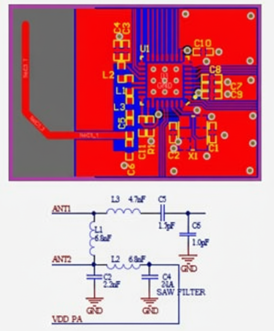
Figure 12: Correct PCB routing and equivalent circuit
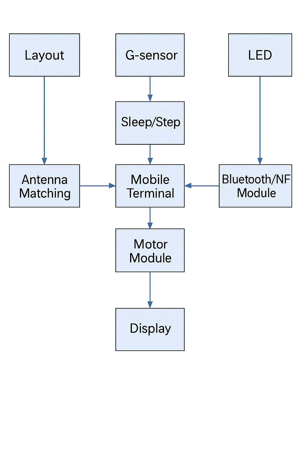
Figure 13: Main program flowchart