Machine vision systems enable automated, non-contact inspection, measurement, and process control in industrial environments. These systems capture and analyze images to deliver quantitative data for quality assurance, robot guidance, and equipment monitoring. In Industry 4.0 manufacturing, machine vision improves speed, repeatability, and accuracy compared with manual inspection while supporting high-throughput production lines.
From a PCB manufacturing perspective, the performance of machine vision depends on the underlying printed circuit boards that integrate sensors, process signals, drive illumination, and run AI algorithms. Proper PCB design addresses signal integrity, thermal dissipation, EMI/EMC compliance, and long-term reliability under industrial conditions.
System Architecture and Key Components
A typical machine vision setup consists of image acquisition hardware, processing units, and decision-making interfaces. Image acquisition includes the light source, lens, camera, and associated electronics. Processing relies on industrial computers or embedded modules running vision software. Output interfaces trigger mechanical actuators or generate pass/fail signals.
PCBs form the backbone of each subsystem. Camera PCBs must support high-resolution sensors with precise timing and low-noise analog-to-digital conversion. Illumination PCBs drive LEDs or structured-light sources while managing heat and current. Processing boards handle high-speed data transfer and complex algorithms. Material choices such as high-Tg FR4 or specialized laminates ensure stability across temperature variations and mechanical stress.
Industrial Area-Scan Cameras: Sensor Technology and PCB Integration
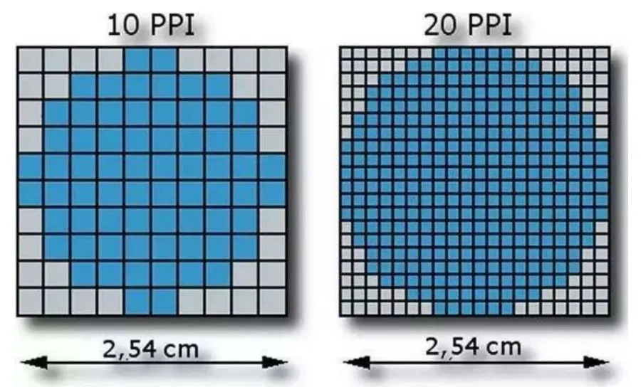
Area-scan cameras capture complete two-dimensional images in a single exposure, making them suitable for most static or slow-moving inspection tasks. They are classified by sensor type—CCD or CMOS—and by charge-transfer architecture, including interline transfer, frame transfer, and full-frame designs.
Key performance parameters directly influence PCB requirements:
- Pixel size and array resolution determine the density of traces and vias needed for sensor interfacing.
- Frame rate and readout speed demand high-speed serial interfaces such as Camera Link, GigE Vision, or CoaXPress on the HDI PCB.
- Quantum efficiency and exposure control require stable power delivery networks and low-noise grounding schemes.
- Readout rate considerations affect PCB stack-up for controlled impedance and minimal crosstalk.
CMOS sensors have largely replaced CCDs in modern designs due to lower power consumption and higher integration, allowing more compact camera PCBs with integrated processing. In electronics manufacturing, food processing, automotive assembly, and logistics, these cameras detect defects, measure dimensions, and guide robots. PCB layout must accommodate the sensor's output bandwidth while maintaining signal integrity over industrial cable lengths.
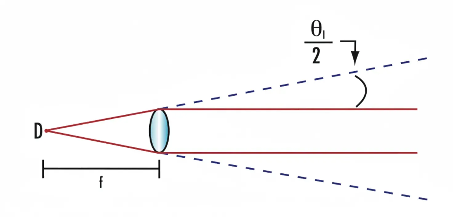
Lens Selection and Optical Performance
The lens determines field of view, magnification, and image sharpness. Critical parameters include focal length, aperture (f-number), distortion, astigmatism, and resolution measured in line pairs per millimeter. System resolution is limited by the weaker of the optical or sensor resolution, so lens choice must match sensor pixel pitch.
PCB-level implications arise in autofocus or motorized zoom mechanisms, where driver circuits and feedback sensors reside on dedicated boards. Interface standards (C-mount, CS-mount, F-mount) influence mechanical and electrical integration. Sensor format matching prevents vignetting and ensures uniform illumination across the image plane. For high-resolution applications, lenses capable of resolving several megapixels require PCBs with fine-pitch connectors and careful impedance control to preserve edge sharpness.
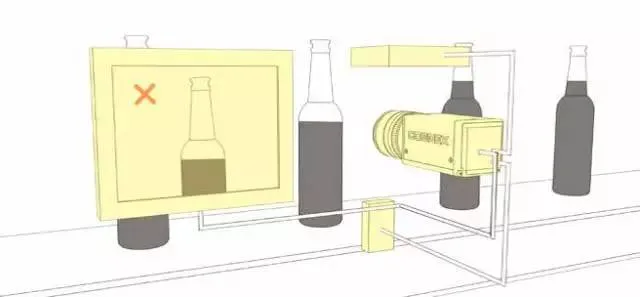
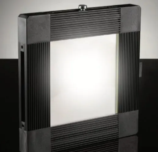
Contour Lighting for Precise Edge Detection
Accurate edge and contour measurement requires controlled illumination that minimizes scattering. Traditional backlights, masked backlights, collimated backlights, and telecentric illuminators each present different trade-offs in divergence, numerical aperture matching, and edge contrast.
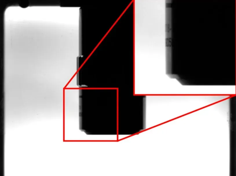
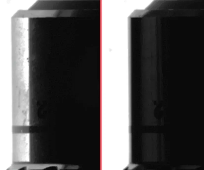
Telecentric illuminators paired with telecentric lenses deliver the sharpest contours by producing near-parallel rays and matching the imaging lens numerical aperture. This reduces edge blur from a few dozen pixels (typical of divergent sources) to just a few pixels, improving measurement repeatability.
Lighting PCBs must deliver precise current to LED arrays or laser sources while incorporating thermal vias, heat sinks, or metal-core substrates to maintain wavelength stability. Collimation films or custom optics add mechanical constraints that affect board layout. In high-precision metrology, stable drive electronics on the illumination PCB directly determine the quality of the captured contour data.
AI-Enhanced Image Recognition: Belt Conveyor Monitoring Case Study
Machine vision combined with AI extends beyond simple pass/fail inspection to predictive monitoring. In coal-fired power plants, belt conveyors experience misalignment, cracking, tearing, spillage, and foreign-object intrusion. An intelligent system using network cameras and structured-light contouring detects these faults in real time.
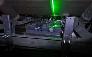
Implementation typically includes:
- Line-scan or area-scan cameras (often 2K resolution or higher) with short exposure times to freeze motion at belt speeds up to 3 m/s.
- Laser emitters projecting contour lines across the belt width.
- High-performance compute servers or edge AI modules running gradient-based line extraction and deep-learning classifiers.
- Alarm outputs that can trigger automatic shutdowns.
The PCBs in these systems must support:
- High-frame-rate data acquisition with minimal latency.
- Robust power conditioning for explosion-proof or harsh environments.
- Accelerated inference hardware (FPGAs or AI accelerators) with adequate thermal management.
- Secure network interfaces for centralized monitoring and mobile alerts.
By replacing manual inspections, such systems reduce belt replacement frequency, prevent catastrophic failures, and improve personnel safety.
PCB Engineering Best Practices for Machine Vision Reliability
Successful deployment requires attention to several PCB-level factors:
Signal Integrity and High-Speed Design — Camera data paths often exceed 1 Gbps. Controlled-impedance traces, proper via stitching, and differential pair routing are essential. Stack-up optimization minimizes crosstalk between analog sensor signals and digital processing lines.
Thermal Management — LED illuminators and high-performance processors generate significant heat. Copper thickness, thermal vias, and metal-core or ceramic substrates help dissipate heat without compromising board reliability.
EMI/EMC Compliance — Industrial environments contain motors, variable-frequency drives, and switching power supplies. Ground planes, shielding cans, and filtered power inputs on the PCB reduce susceptibility and emissions.
Material and Reliability — High-Tg laminates, halogen-free materials, and conformal coating protect against humidity, vibration, and temperature cycling. Via-in-pad technology and fine-line capabilities support dense sensor integration.
Manufacturing Considerations — Panelization, fiducial placement, and test-point accessibility affect yield during volume production. Early involvement of the PCB fabricator ensures stack-up compatibility with high-speed materials and fine features.
Conclusion
Machine vision systems deliver measurable improvements in inspection speed, accuracy, and automation. Their effectiveness ultimately depends on the quality and integration of the supporting PCBs. By addressing signal integrity, thermal performance, material selection, and manufacturing constraints from the design stage, engineers can create robust, high-performance vision platforms suitable for demanding industrial applications.
Aivon's expertise in advanced PCB manufacturing supports the specialized requirements of machine vision hardware—high-density interconnects, controlled-impedance boards, thermal solutions, and reliable assembly—helping customers bring precise, dependable vision systems to market.