Contour Lighting in Machine Vision: Methods and Implementation
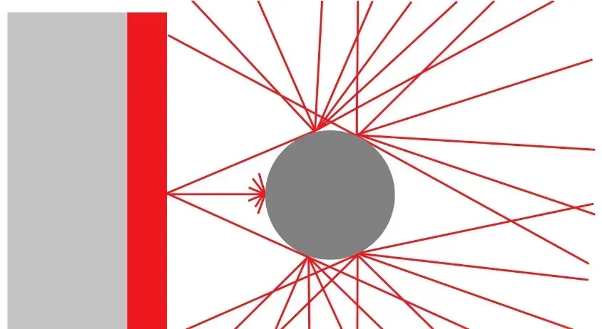
Compare occlusion lighting: traditional, masked, collimated backlights and telecentric illuminators, analyzing divergence, numerical aperture, edge contrast and trade-offs for inspection.