Array Repair
Array Repair addresses open-circuit or short-circuit defects that occur during the manufacturing of LCD/OLED arrays (G6, G8.5, G8.6, G10). These defects can be repaired using laser cut and CVD techniques.
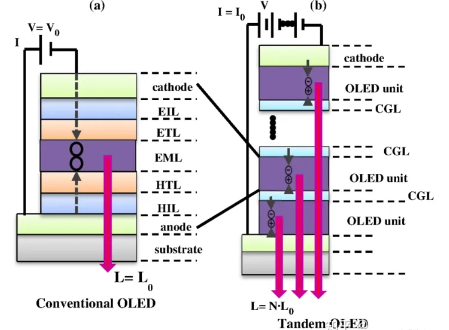
Tandem OLED
Tandem means "stacked in series." Compared with conventional OLEDs, tandem OLEDs stack multiple electroluminescent devices for each pixel, connected through intermediate layers. These intermediate layers are composed of mixed p-type and n-type materials, so electrons and holes injected from the two electrodes are separated across the connection layers, allowing the stacked OLED devices to be driven.
As an analogy, a conventional device is like a single dry cell; a tandem device is like several dry cells connected in series, increasing the effective drive for light emission.
De-Burn-in
With OLED materials, prolonged operation leads to material aging and reduced efficiency. The decay rates for R, G, and B differ, causing brightness loss and, in severe cases, color shift. Although this decay is usually slow and hard for users to notice, certain scenarios require attention:
- Higher pixel density per unit area (higher PPI) leads to more noticeable lifetime degradation as pixel area shrinks.
- Foldable smartphones can show brightness inconsistency between full-screen and half-screen usage patterns.
- Prolonged viewing of small gray-scale regions, common in short-form video apps, can cause image retention.
Short-term brightness inconsistency or long-duration static images, caused by driving TFT characteristics, can be compensated by the DDIC using ODC (overdriving compensation). Long-term brightness decay is handled by de-burn-in compensation, which also helps reduce image retention.
De-burn-in requires collecting parameters such as time, brightness, gray level, image content, temperature, and frame rate. These parameters are stored in the panel flash IC. During compensation, the DDIC reloads the parameters from the flash, looks up compensation gains, and adjusts gamma to output the target compensated brightness.
The most challenging tasks are table lookup and gain calculation. Panel manufacturers must collect data and build compensation models, considering consistency across the panel. Different projects, emissive materials, or panel designs require separate models.
There are three target brightness strategies used by DDIC vendors:
- Raise both weaker and stronger aged areas up to the original initial brightness.
- Raise the strongly aged region to match the weakly aged region.
- Lower the weakly aged region to match the stronger aged region.
All three approaches aim to maintain uniform brightness across the display. The screen can be divided into blocks and compensated toward a chosen target block or the initial brightness.
Strategies 1 and 2, commonly adopted by Chinese DDIC suppliers, increase brightness. Their main drawback is that they accelerate aging by maintaining higher drive currents, which can speed up device degradation. Strategy 3, a compensation method seen from a Korean supplier and already deployed in production, reduces brightness to match the lower area. This approach maintains uniformity while effectively extending OLED lifetime. When brightness decays to a certain fraction of initial brightness (for example, 85%), de-burn-in can be disabled to avoid perceptible brightness loss for the user.
Overall, strategy 3 appears preferable as a short-term mitigation. However, the fundamental solution remains improving emissive material lifetime and addressing TFT hysteresis.
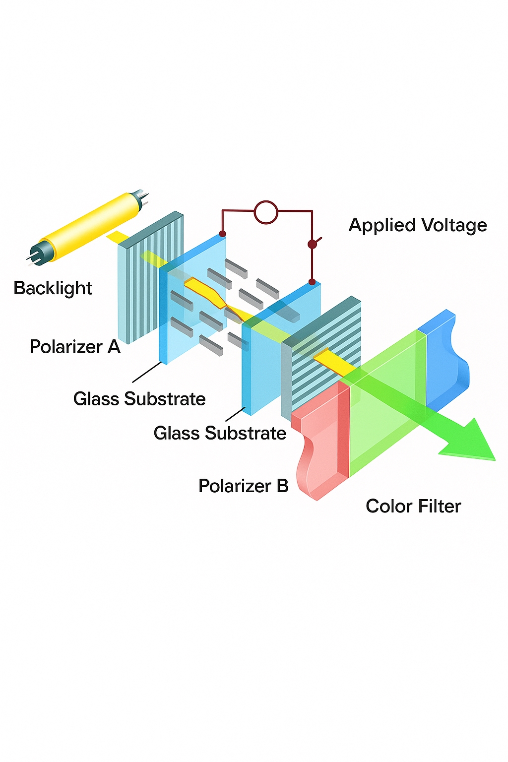
Demura
Demura compensates for brightness nonuniformity (mura) caused by panel structure or process variations, making the image more uniform. The method acquires per-pixel brightness information and computes compensation values to add to or multiply with the original image to remove luminance deviations.
Typical Demura workflow:
- Camera capture
- Image processing
- Generate compensation data
- Downloading and driving
TCON
Every display panel requires a timing controller (TCON). The TCON converts standard video signals into the specific row and column driving signals required by the display panel and sends them to the panel DDICs. The display panel responds optically to the incoming charge, which must be refreshed continuously; otherwise, the response decays. Therefore, precise timing is required to refresh the panel properly, and this is the TCON's role.
More specifically, a computer display TCON receives RGB data from the GPU, processes the signals, and forwards them to the DDIC (source IC/gate IC). The TCON provides timing control that the DDIC does not. For example, a 1920x1080 LCD may have 1920*3 source channels and 1080 gate rows, requiring 5760 source driver channels and 1080 gate driver channels.
The TCON issues different control signals for these drivers, such as POL for switching liquid crystal polarity, STH for initiating input line pulses, LOCK to notify the source driver that all row signals have been received, and the RGB data itself.
The TCON also manages power, backlight, FRC, gamma adjustment, and other functions. As modern panels increase in resolution, refresh rate, color gamut, and color depth, the TCON's processing capability and interface bandwidth face growing challenges.
COP and COF Packaging
COP, or Chip On PI, is a packaging technique tailored for flexible OLED screens. It folds part of the display and integrates the display flex cable and IC under the screen. COP enables near-bezel-less designs but is typically used in higher-end devices due to cost.
COF, or Chip On Film, integrates the display ICs on a flexible PCB film that is bent under the display. COF reduces bezel width and increases screen-to-body ratio. Many mid- to high-end full-screen and notched phones use COF packaging.
Both COF and COP are applicable to flexible OLEDs. COP can further fold the backplane over COF to minimize the bottom bezel, but COP is generally used in premium devices for economic reasons.
CUP (Camera Under Panel)
Camera Under Panel aims for truly full-screen displays by placing the camera beneath the OLED. If the display stack is reduced to the bare glass and light-emitting layers, measured light transmittance can be below 6%, indicating that the OLED stack is not very transparent.
To allow normal display when not photographing and higher transmittance during camera operation, a low-PPI technique is used. By reducing pixel density in the camera area (for example, from 400 PPI to 200 PPI), the open area for light increases, improving transmittance. Low-PPI was initially proposed by JDI and has been developed by various OLED suppliers.
Low-PPI implementations include:
- Single-panel: lower resolution in the camera region.
- Popup mini-panel: a low-PPI small panel dedicated to the camera area.
OLED manufacturers optimize routing to avoid the camera hole and have pushed panel transmittance from about 6% to nearly 50%. Further improvements are increasingly difficult and also require better camera sensor sensitivity.
MLP (Micro Lens Panel)
MLP micro-lens technology fabricates microscopic lenses over each OLED subpixel via photolithography. By introducing high-refractive-index materials, emitted light is refracted at the lens interface to focus more light toward the display normal. An array of millions of micro-lenses concentrates light that would otherwise scatter toward the sides, increasing on-axis brightness without raising total emitted power.
TCL Huaxing's MLP uses pixel-level patterned arrays and refractive index layering to increase forward light output, improving brightness and reducing display power consumption.
TFP (In-Display Fingerprint)
In-display fingerprint solutions for OLED have three main variants:
- Ultrasonic fingerprint, led by Qualcomm, which supports IP68 dust and water resistance and can operate underwater. It also supports liveness detection via heartbeat and blood flow sensing, making fake fingerprints ineffective.
- Collimator-based optical approach, used in early in-display fingerprint phones, embeds an optical sensor under the OLED and uses micro-lenses to collect light passing through a small display opening to form the fingerprint image.
- Under-panel camera approach, which replaces the fingerprint sensor with a special camera module (fingerprint IC, ultra-short-focus CMOS fisheye camera, light sensor, NOR flash, and filter). This "CMOS solution" captures and matches fingerprint information via an under-display camera.
BSM (Back Side Metallization)
BSM, or back side metallization, is a physical vapor deposition (PVD) process in which metal is deposited on the thinned chip backside. Back side metallization reduces thermal resistance, improving heat dissipation. Some power devices use a backside electrode to provide good ohmic contact and reliable soldering, boosting product reliability.
Advantages: allows alloy evaporation and simple control.
Disadvantages: source material must be replenished for each evaporation, and film density and uniformity can be poor.
FIAA
FIAA transfers fanout routing into the active display area to save fanout routing space in the bottom bezel, narrowing the bottom bezel by at least 20% and increasing display area while maintaining image quality.
The fanout region connects TFT panel signal pins to the PCB-mounted ICs for signal transmission. To preserve SMD placement quality, vias are typically avoided on SMD pads; instead, fanout routing extends traces from the SMD pad to a via. For high-pin-count components such as BGA, fanout routing is commonly used. However, this method has signal transmission risks, and achieving very narrow bezels requires trade-offs.
FMM (Fine Metal Mask)
FMM is fine metal mask technology used in vacuum deposition processes for AMOLED mass production. In vacuum evaporation, FMM masks separate RGB emissive materials into narrow pixel regions. For large-size panels, mask deformation and material overuse are challenges; maintaining surface flatness is a key precision requirement.
Invar, a nickel-iron alloy with low thermal expansion coefficient and high stiffness, is often used for FMM to mitigate thermal bending and misalignment issues during large-panel processing.
LTPO
LTPO, Low Temperature Polycrystalline Oxide, enables adaptive refresh rate control for OLED panels, addressing display power consumption. LTPO merges features of LTPS and IGZO to create a faster response with lower power consumption by adding an oxide layer that reduces the energy required to excite pixels.
LLO (Laser Lift-Off)
Laser lift-off removes a device layer by ablating material with pulsed laser irradiation, enabling transfer of devices to a flexible substrate. Compared with chemical etching, mechanical peeling, or ion beam removal, laser lift-off offers higher energy efficiency, lower device damage, open equipment architecture, and flexible application. LLO is a key process for flexible electronics.
Flexible OLED displays use flexible PI film as the substrate with glass as a carrier. Laser lift-off is a critical process to separate the PI substrate from the glass carrier.