Hardware supplement
Yesterday I posted an overview of an ESP32 open-source oscilloscope. This article provides the hardware design details.
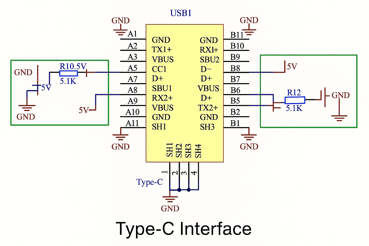
Type-C interface and identification resistor
Note that the Type-C identification resistor is 5.1 kΩ.
Electronic switch and package
I selected an electronic switch component as the switching element.
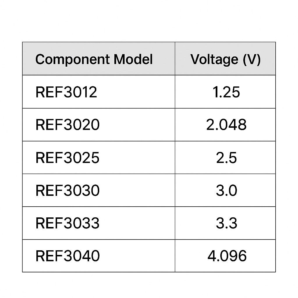
Package: 3012
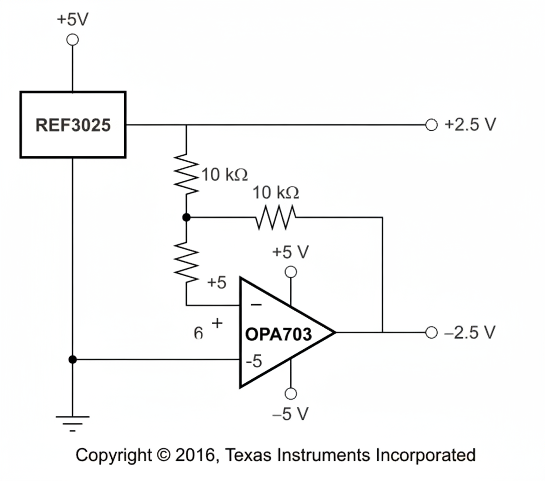
Negative supply generation
A low-offset OPA703 can be used to generate a negative voltage.
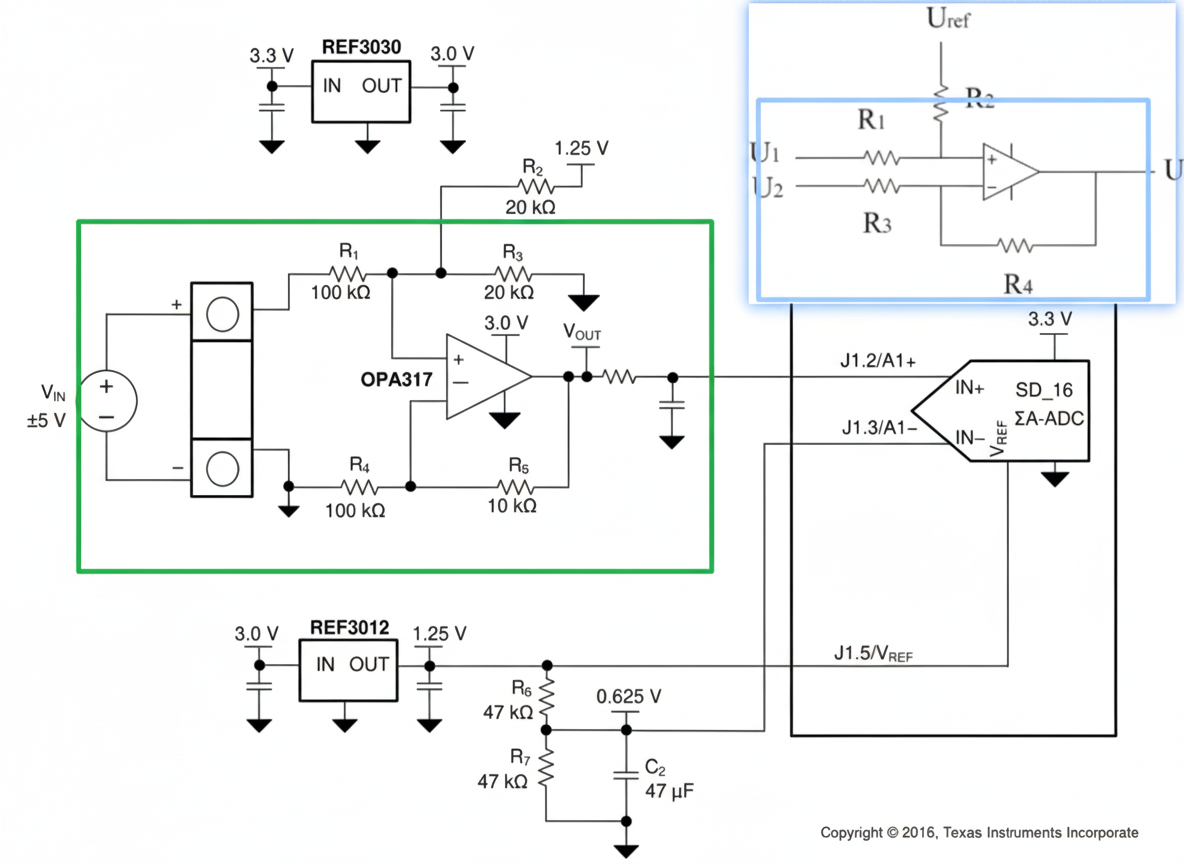
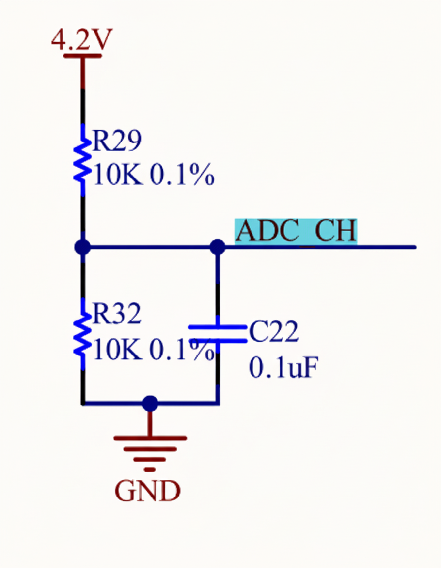
ADC input and input conditioning
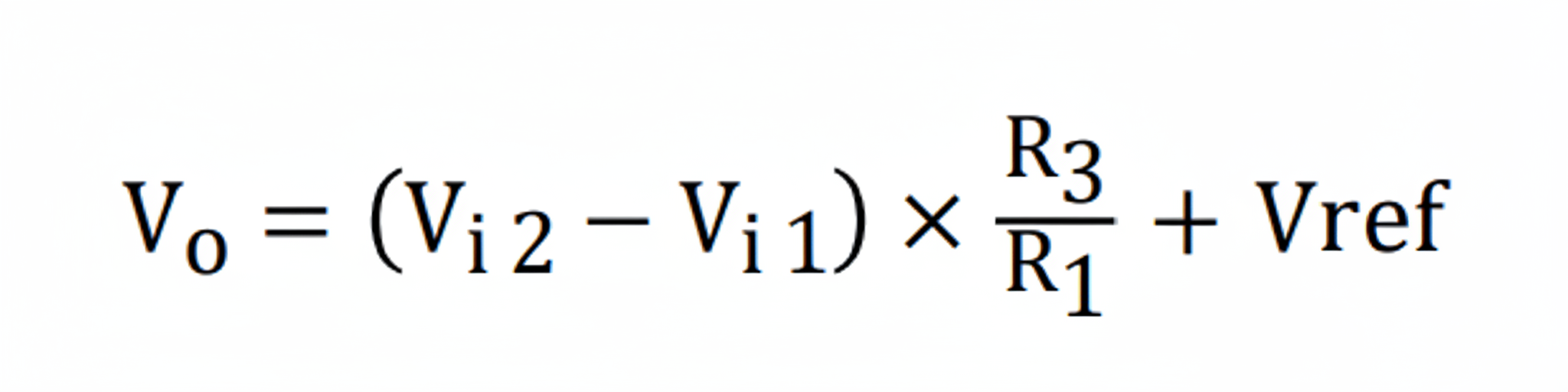
The ADC input and full input conditioning circuit are shown here. The ADC is configured for bipolar measurements: the final conversion result is the differential voltage between the positive and negative ADC inputs. Bipolar GND-referenced signals must be level-shifted and attenuated by op amps so that the outputs are biased at VREF/2 and their differential voltages remain within the ADC input range of ±VREF/2.
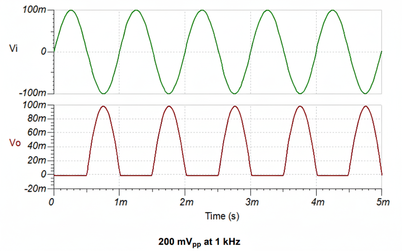
Precision rectifier: single-T topology
This precision rectifier is the single-T topology: AC in, DC out. A small AC signal is first processed by a half-wave rectifier stage that produces a half-wave signal. That signal is then combined with the input in the following stage to produce a full-wave rectified output. This implements rectification of small AC signals.
The single-op amp rectifier can achieve rectification but has poor input/output characteristics. Buffer stages or non-inverting amplifiers are needed at the input and output for isolation, which explains the presence of a follower at the front of the schematic.
The precision half-wave rectifier inverts the negative half of a time-varying input signal (ideally a sine) and passes it to the output. By selecting feedback resistors appropriately, different gains are achievable. These rectifiers are typically used with other op amp circuits, such as peak detectors or bandwidth-limited non-inverting amplifiers, to produce a DC output. This configuration is designed for sine inputs from 0.2 mVpp to 4 Vpp, at frequencies up to 50 kHz.
Switching control
Another switch is used here: the 2.5 V reference is treated as the 0 V reference, and K4 selects the measurement resistor.
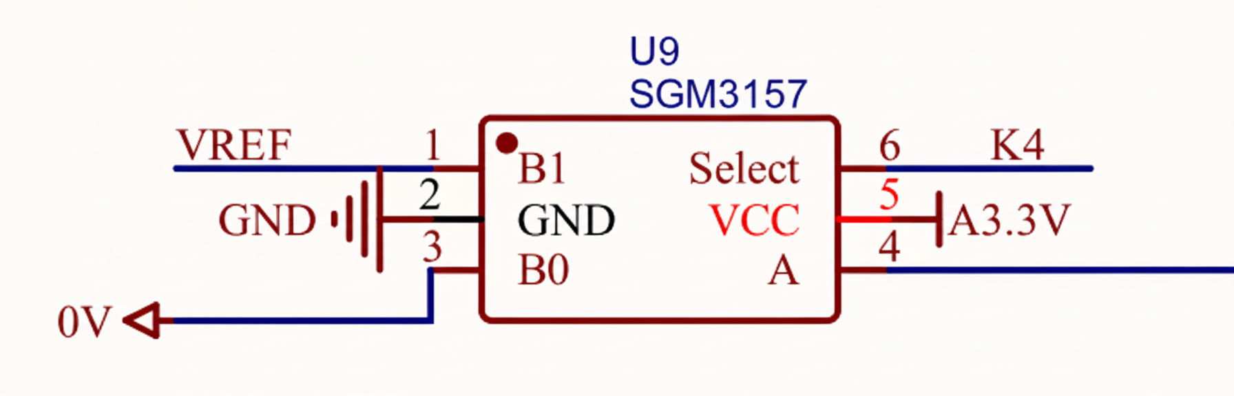
The switch arrangement is vertical. Different resistors are selected depending on the switch position. When the resistor is connected it forms a divider with the reference resistor.
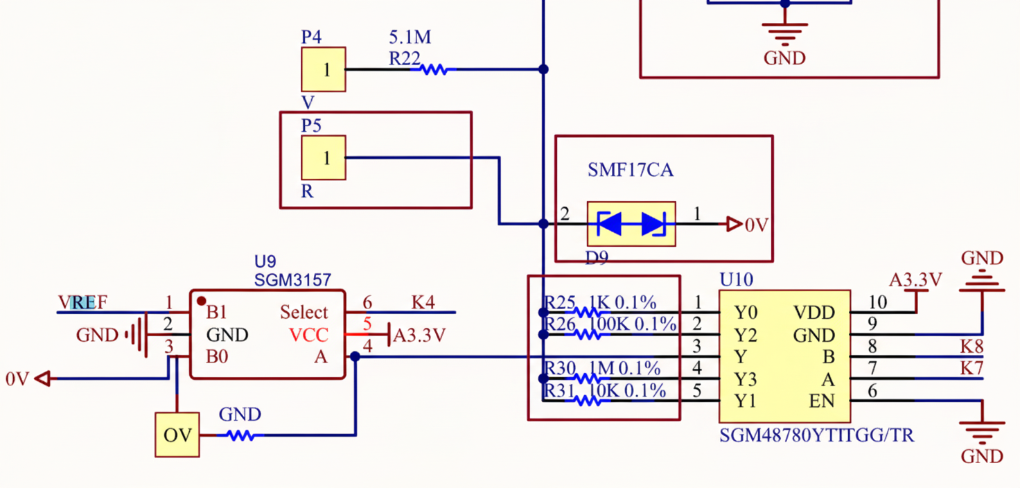
The signal then routes through the top switch; the upper and lower switches are mirrored, followed by a two-pole switch and a buffer to preserve signal integrity.
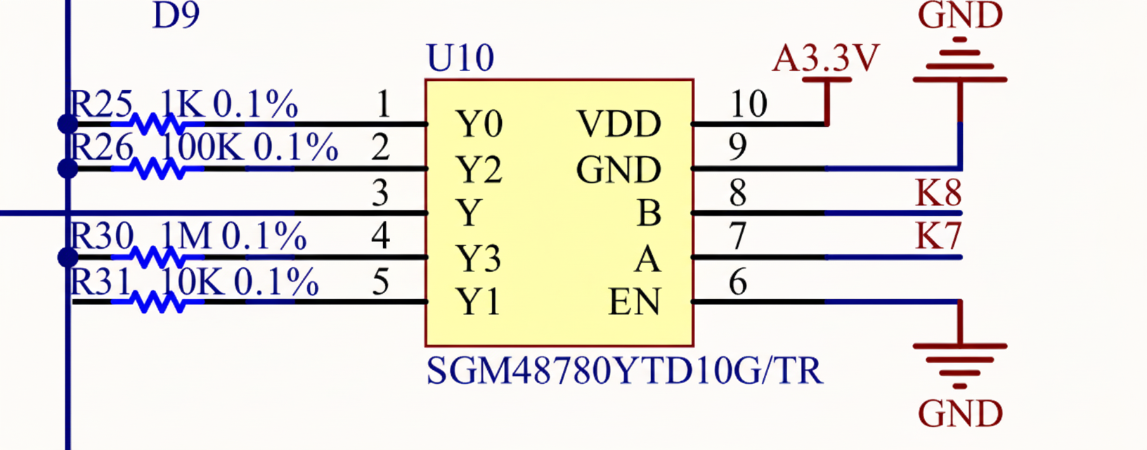
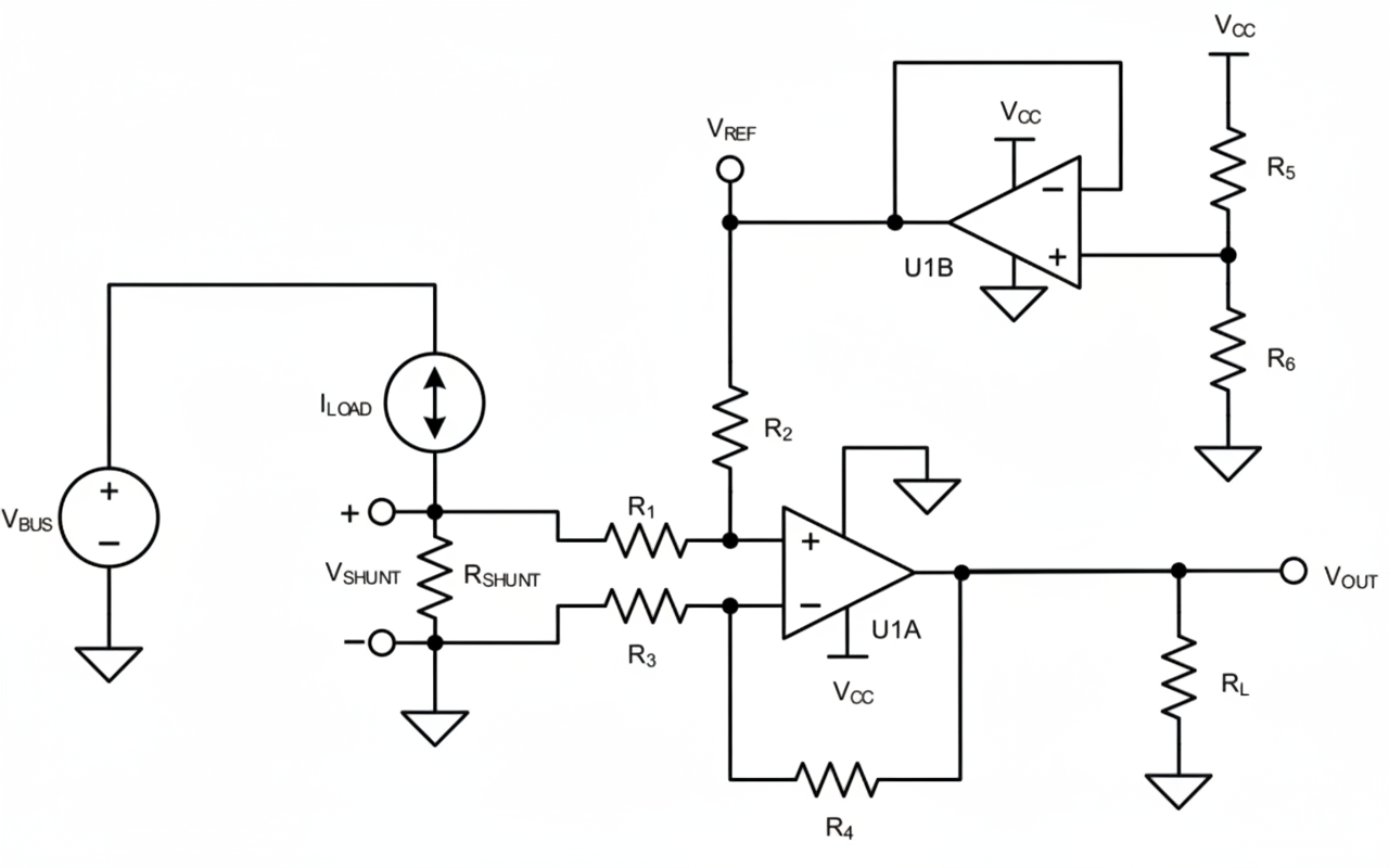
ADC front end and current measurement
Bypassing capacitors are used before the ADC.
A parallel shunt resistor is used to extend the current measurement range. Changing the shunt resistance changes the current measurement range.
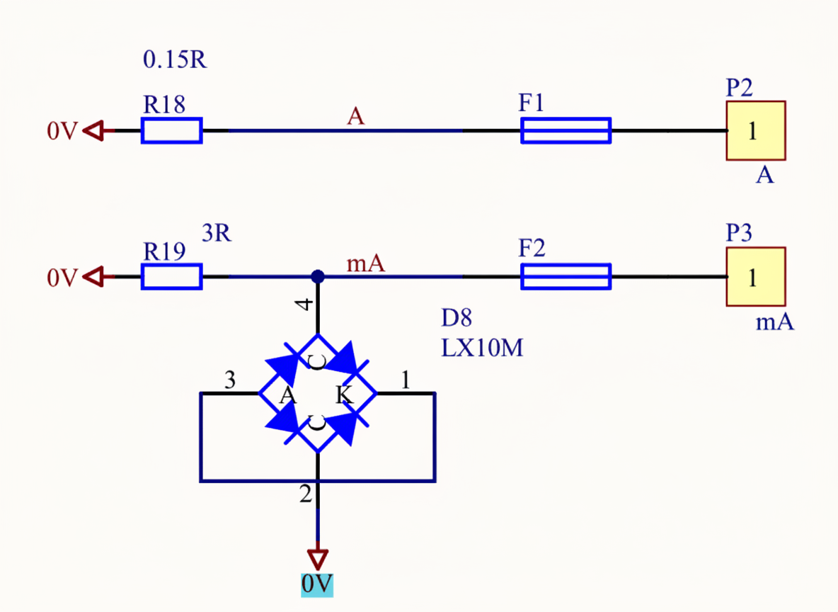
It was initially unclear why a 0 V reference was used; the following section clarifies this.
Rectifier bridge and ADC buffering
The rectifier bridge is connected here and is routed directly to a buffer and then to the ADC.
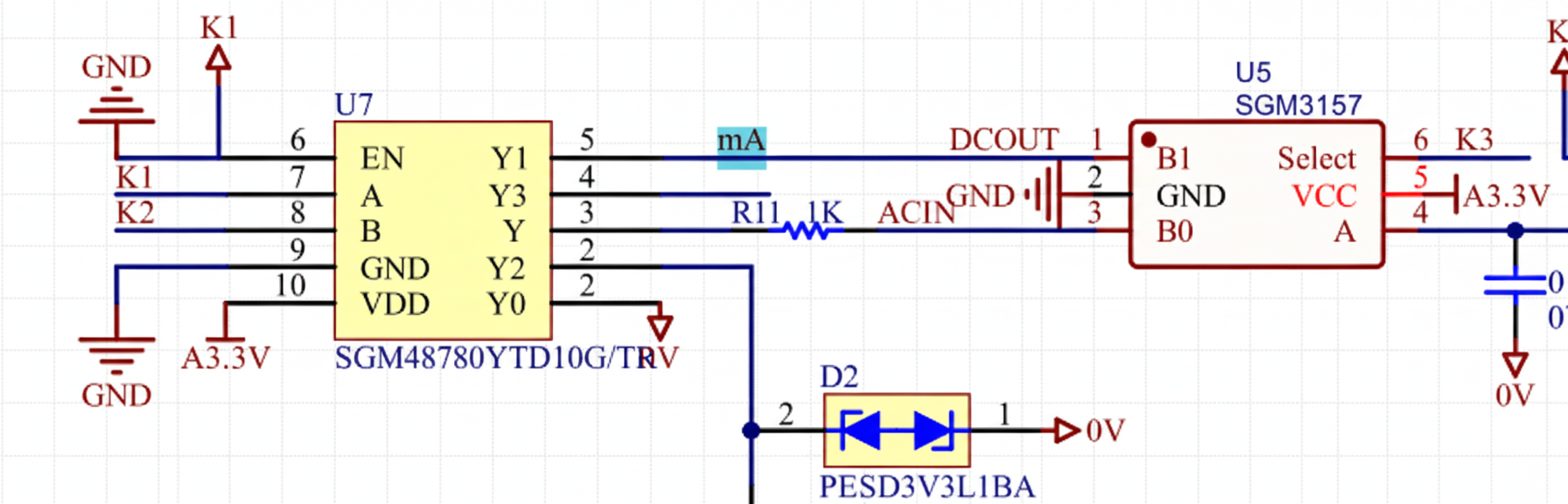
This node computes to approximately 2.1 V and is supplied to the ADC.
Virtual ground and buffering
Single-supply op amps require a virtual ground, typically VCC/2. The shown circuit can generate VCC/2 but reduces the system low-frequency performance. R5 and R7 are equal; the overall stage functions as a buffer.
I will run a simulation later to verify the capacitor's role in this circuit.
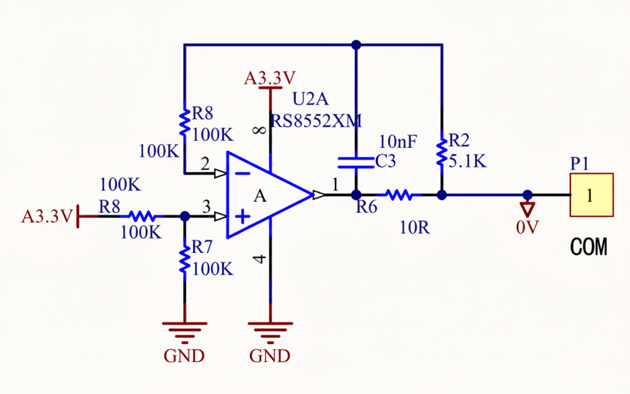
Op amp selection and application
The op amp used is a Jiangsu Runshi precision device. In addition to low offset voltage, it provides CMOS rail-to-rail inputs and outputs. The design shown implements a differential stage plus a reference channel.
The given application is bidirectional current sensing: a single-supply, low-side, bidirectional current sensing solution that detects load currents from -1 A to 1 A. The single-ended output range is approximately 110 mV to 3.19 V. The design uses the RS855X because of its low offset and rail-to-rail I/O characteristics.
Layout and next steps
Layout examples are provided. This article has presented a brief circuit analysis. The next article will summarize the design choices in more detail, followed by the software implementation.