Overview
According to Mems Consulting, Israeli manufacturer Semi Conductor Devices (SCD), which produces uncooled infrared detectors and high-power laser diodes, has introduced a new event-based shortwave infrared (SWIR) detector called Swift-El.
Design and imaging architecture
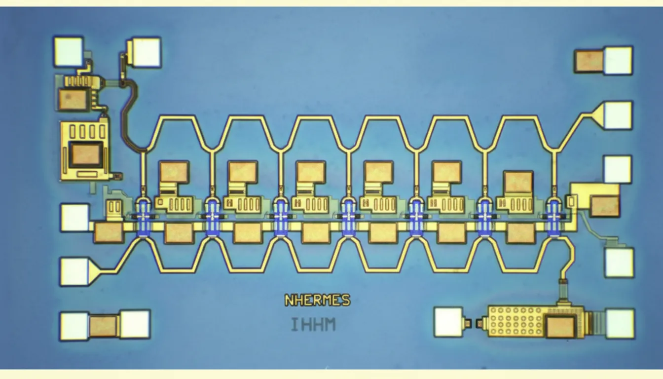
Swift-El is a VGA-format SWIR detector with a 10 μm pixel pitch, engineered for low size, weight, and power (SWaP) and low cost. SCD describes Swift-El as the first SWIR detector to integrate event-based imaging functionality, making it a notable addition for defense and industrial use.
Its focal plane array (FPA) detection capabilities enable tactical units to detect multiple laser sources, laser spots, hostile fire indicators (HFI), and similar signatures. The detector's readout integrated circuit (ROIC) imager provides two parallel video channels on a single sensor: a standard imaging SWIR video channel and an ultra-high-frame-rate event imaging channel.
Features and applications
Swift-El supports SWIR imaging in daylight and low-light scenarios, enabling all-weather situational awareness and improved atmospheric penetration while providing lower-cost SWIR imagery for tactical applications. The event-based imaging channel supports functions such as laser event spot detection, multi-laser-point LST capability, and event-based SWIR imaging, expanding target detection and classification capabilities.
The detector also targets machine vision applications, including production line sorters and smart agriculture, where advanced SWIR image analysis is required for automated decision-making. Swift-El can deliver full-frame rates exceeding 1200 Hz, which is important for machine vision and AI algorithms.
Specifications and production
Swift-El has a resolution of 640 x 512 with a 10 μm pixel pitch. It is manufactured at the company's wafer fab in Israel and is aimed at defense and industrial markets, with production planned for 2024.
Manufacturing and scale
Shai Fishbeing, vice president of business development and marketing at SCD, said the company focuses on economies of scale to increase capacity and yield, and operates one of the largest thermal camera manufacturing facilities.