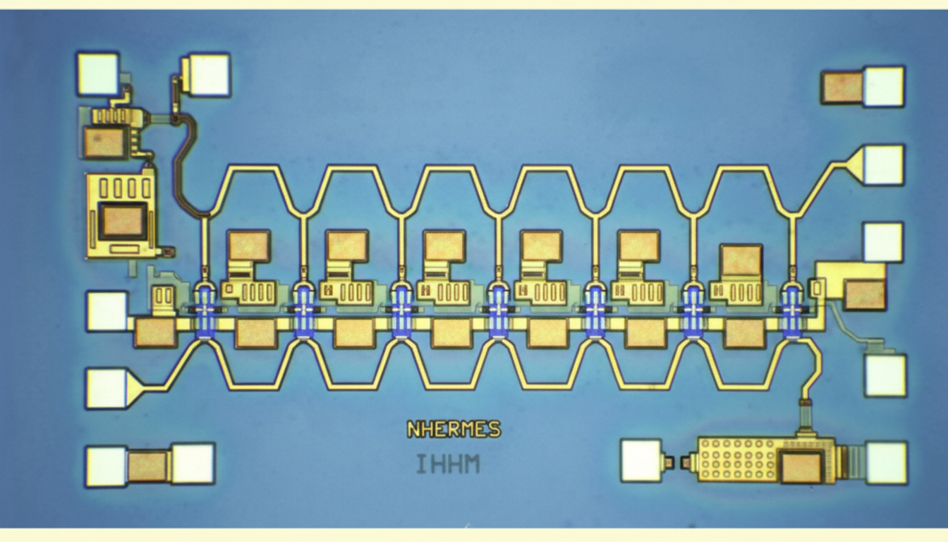
Planar waveguide delay lines offer compact size and easy integration. Waveguide length can be precisely modulated to control delay time, and very long waveguide traces can be fabricated, making them useful in silicon photonic integrated chip systems.
OFDR instruments offer spatial resolution as high as 10 um and can rapidly and accurately characterize on-chip optical paths. This article uses a high-resolution optical link diagnostic instrument (OCI) based on OFDR principles to measure a planar waveguide delay line, diagnosing insertion loss, return loss, distances, and other information at sub-millimeter resolution.
Conclusion
The waveguide length, waveguide loss, and return loss at the coupling locations determine the quality of a planar waveguide delay line. OCI equipment can scan on-chip optical links at sub-millimeter resolution to obtain return loss at each point and characterize the entire optical path. These precise optical measurements provide useful data for silicon photonic chip researchers.


