Introduction
The oscilloscope is the essential instrument for electronics engineers and technicians. Probes are often marked X10, X100, etc. What do these attenuation factors mean? If you only follow the user manual, how does that differ from a repair technician? This article explains the underlying principles so you can use probes more flexibly in practice.
Oscilloscope input and probe structure
The oscilloscope input stage contains a vertical amplifier with a very high input impedance. Typical selectable input resistance on oscilloscopes is 1 MΩ (the 50 Ω setting is used for impedance matching with high-frequency communication signals). The input capacitance is commonly about 20 pF.
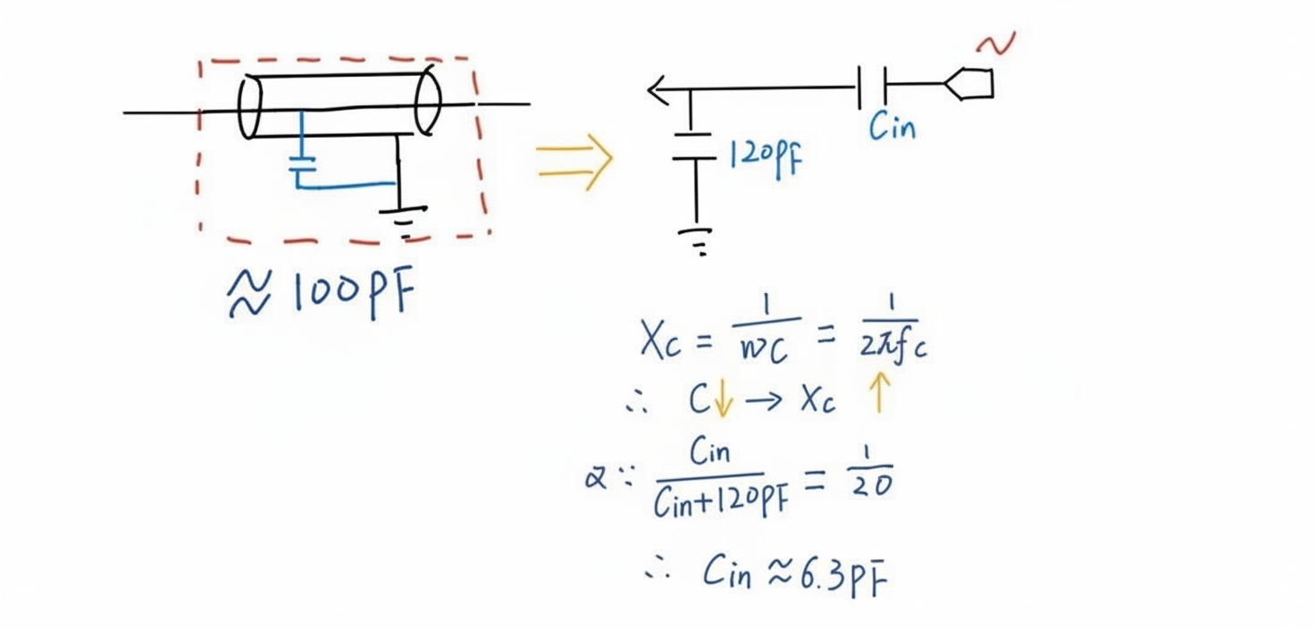
For a probe such as a X20 probe, the probe tip typically contains an RC network (shown in the dashed box) arranged so that resistance and capacitance can be adjusted. The probe cable is shielded; the shield tied to ground forms an equivalent capacitance of roughly 100 pF between the shield and the probe conductor. How does the oscilloscope and probe adjust R and C so the input signal is attenuated by 20 dB before entering the scope? The following analysis explains this.
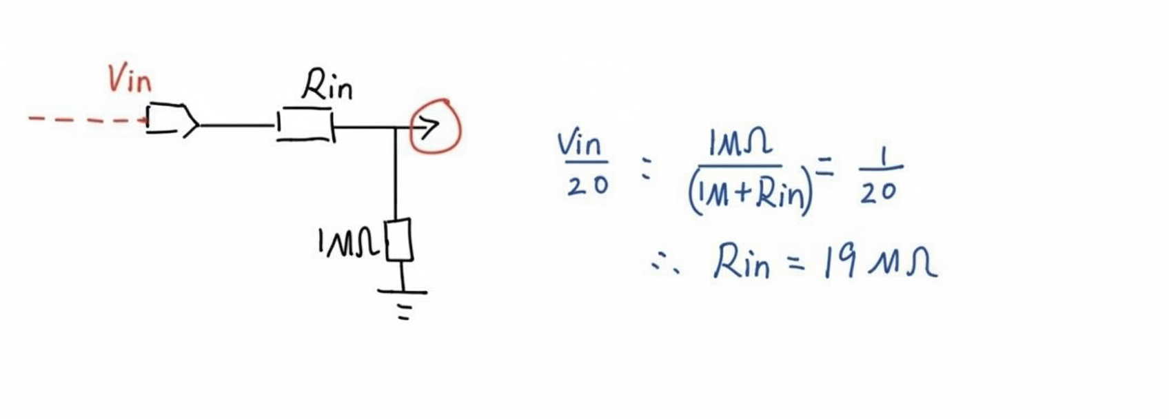
AC and DC behavior
- For AC signals: Using the equivalent circuit, the capacitive divider formed by the probe input capacitance Cin to ground in series with the probe cable plus the oscilloscope input capacitance (about 120 pF total) determines the AC attenuation. From the capacitive reactance relationship, the ratio of Cin to the input equivalent capacitance must be 1/20 to achieve 20 dB attenuation. Solving gives Cin ≈ 6.3 pF.
- For DC signals: The DC behavior is a resistor divider between the probe resistor Rin and the oscilloscope input resistance. To obtain 20 dB attenuation, Rin should be set to about 19 MΩ.
Calibration and simulation
- Adjustable RC calibration: For the resistor Rin, a precision resistor provides accurate DC attenuation. The capacitance must be calibrated to get the correct AC gain. Oscilloscopes provide a 1 kHz reference square-wave calibration output. When the probe is connected and the displayed square wave is accurate and undistorted, the probe Rin and Cin are at appropriate values and the probe is properly compensated.
- Circuit simulation: A circuit simulation was used to validate the X20 probe design. In the simulation, the oscilloscope vertical amplifier input was modeled as a very large resistance (a 1000 GΩ resistor). A 1 kHz square wave with ±200 V amplitude was applied as the calibration signal. The simulated oscilloscope display shows an undistorted 10 V amplitude square wave, matching the calculation.
Changing Cin to 3 pF produces a clearly distorted output waveform, demonstrating the effect of incorrect capacitance adjustment on probe compensation.
Summary
This note covered the basic principles of oscilloscope probes and a brief circuit simulation verification. The key points are that DC attenuation is set by the resistor divider and AC response is set by the capacitive divider; proper probe compensation is verified with the oscilloscope's 1 kHz calibration square wave. With these principles, it is possible to understand probe behavior and to perform basic adjustments if needed.