Overview
Developers can already access MCUs in low-power states, shutting down peripherals or the core to reduce system power. For some applications, however, finer-grained control of power consumption is required so that selected subsystems remain powered to support critical functions.
MCU-based power management
Historically, designers used discrete power-management devices to implement precise power control. The ADuCM3029 MCU from Analog Devices integrates many of those capabilities, simplifying the tradeoff between peak performance and minimized power consumption for sensor data acquisition, wearable electronics, and other IoT applications.
Advanced MCUs for power-sensitive applications typically provide features such as frequency scaling that let engineers trade performance for lower power. Low-power modes usually shut down increasing numbers of MCU subsystems until only the minimal circuits required to wake the MCU remain powered. Ultra-low-power MCUs add modes that separately control the power of the core and peripherals for improved power management. In some implementations, peripherals are shut down as a group or managed by automated mechanisms that grant limited control over per-peripheral power allocation.
While MCU power-management options commonly include several low-power modes, switching into those modes often results in a significant reduction in available functionality. In many applications that temporary functional loss is acceptable, but where precise power control is critical, the ADuCM3029 is designed to support more complex power-management requirements in ultra-low-power systems.
Device summary
The ADuCM3029 is based on an ARM Cortex-M3 core and provides 256 KB of ECC flash and 64 KB of configurable SRAM with parity protection. The ADuCM3027 variant offers 128 KB of flash while sharing other features. These devices include a hardware cryptographic accelerator, an 8-channel 12-bit ADC, and multiple digital peripherals including SPI, I2C, UART, GPIO, a synchronous serial port (SPORT), and a 25-channel DMA controller. Active-mode power consumption is typically below 30 μA/MHz, and the device supports fine-grained tuning of performance versus power.
Power tuning and Flexi mode
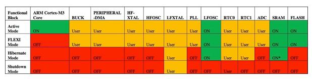
Like most advanced MCUs, the ADuCM3029 provides multiple power modes to reduce consumption during periods of low activity. In sleep mode, the device powers down the processor core and most peripherals while maintaining power to selected SRAM regions, typically consuming less than 750 nA. In the deepest shutdown mode, current can be as low as 60 nA.
Developers often need some peripherals active while the core is idle. To address this, the ADuCM3029 offers a Flexi (flexible sleep) mode. Flexi reduces power to around 300 μA while providing functionality between active and sleep modes. In Flexi mode the core remains asleep while only the developer-specified peripherals remain active. To enter Flexi mode, set the MODE bit in the PMG_PWRMOD register to 0 and execute the WFI instruction. While the core is idle, peripheral clocks can be gated individually by writing 0 to the corresponding bits in the CLKG_CLK_CTL5 register. Although the core cannot execute instructions in this mode, peripherals can continue activities such as DMA transfers between peripherals and memory.
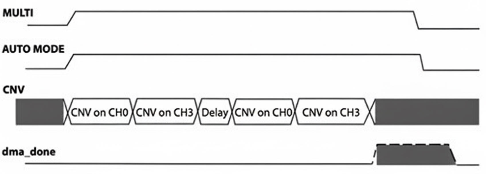
Flexi mode is useful for sensor applications that require sampling one or more sensors for a period before the processor must wake and process the data. The integrated ADC supports automatic cycling on selected channels, and the DMA controller can transfer samples to SRAM. After a programmer-specified number of conversions and DMA transfers, the DMA controller can issue an interrupt to wake the core for data processing (see Figure 1).
Caches and clocks
Flexi and other low-power modes provide powerful mechanisms to reduce peripheral activity and overall system power. For battery-powered systems, designers often need additional power control. Traditional techniques and newer approaches can be combined to further reduce consumption.
Instruction caching reduces accesses to off-chip or high-power on-chip memory such as flash. On the ADuCM3029, up to 4 KB of SRAM can be allocated as a cache. The power savings depend on cache hit rate, but caching can significantly lower power in typical benchmark applications (see Table 2 and Figure 2).
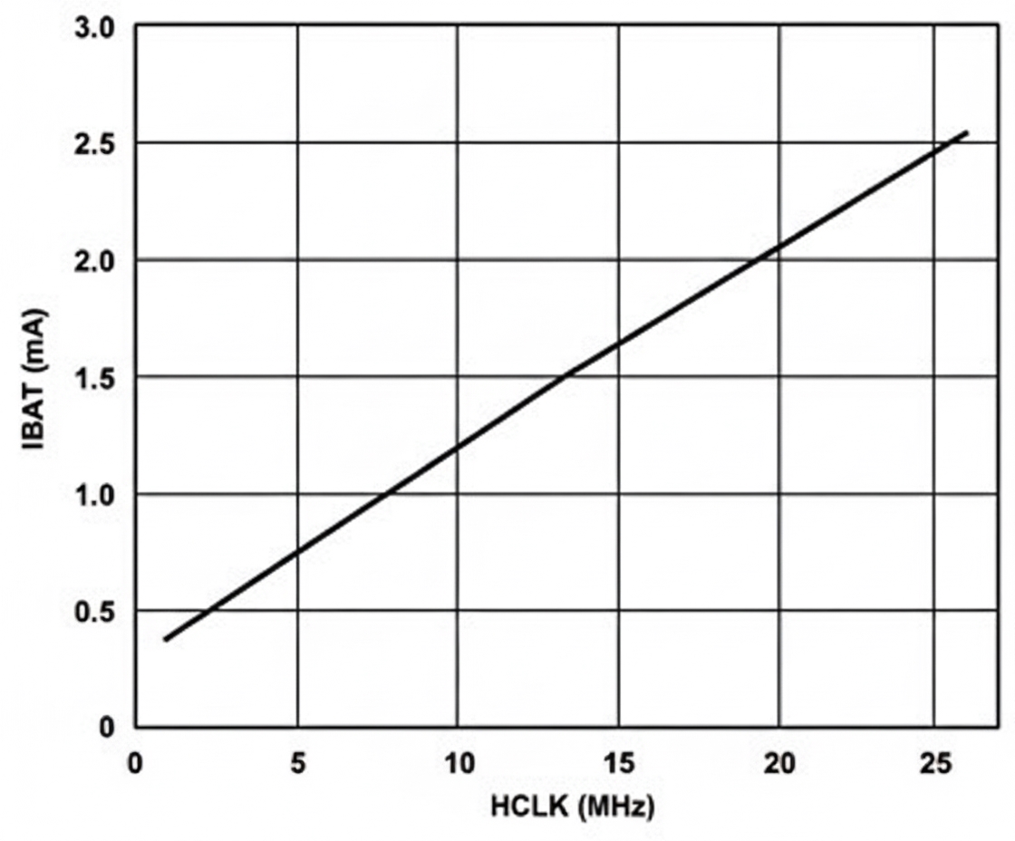
Frequency scaling is another long-term reduction strategy: a lower core clock slows instruction execution while reducing power. Unlike many other MCUs, the ADuCM3029 allows dynamic, independent modification of clock rates for the processor and peripherals. The device uses a PLL and dividers driven by a 26 MHz internal oscillator or external crystal to generate clocks for on-chip resources, while a 32 kHz oscillator or crystal drives the RTC and watchdog/timers. Developers can change clock registers at runtime to adapt performance to changing requirements or to exploit opportunities for power reduction.
Enhanced power path
Beyond traditional system-level techniques, the ADuCM3029 includes on-chip hardware features that enable novel power-reduction methods. The device integrates a buck converter in its power path to reduce the gap between VBAT (1.74 V to 3.6 V) and the internal digital supply (1.2 V).
Under typical operation, an integrated low-dropout regulator (LDO) provides the internal voltage. As with any LDO, when the difference between supply voltage and load voltage is large, the default power path dissipates the excess, resulting in wasted power. With this MCU, a small number of external capacitors enable the buck converter to lower the voltage presented to the LDO at higher supply voltages, reducing power dissipation. Software control enables the buck converter by writing to the PMG_CTL1 register.
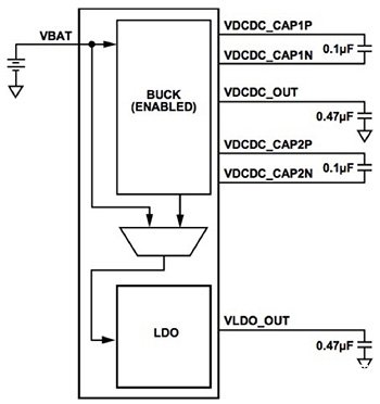
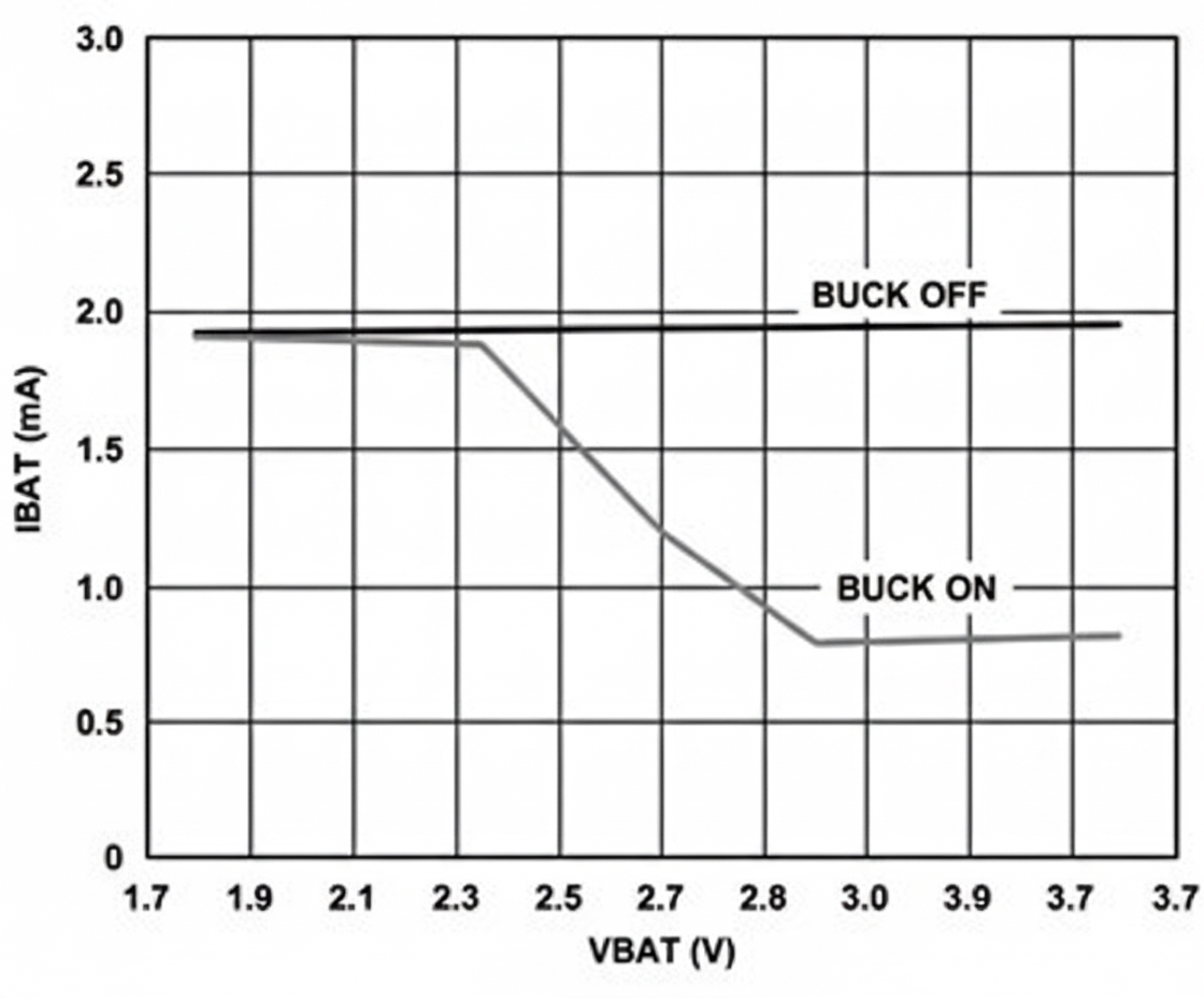
The buck converter uses an efficient capacitor-based charge-pump topology to reduce the voltage supplied to the LDO, significantly lowering power at the upper range of VBAT (see Figure 6). Below approximately 2.3 V, the buck converter bypasses and follows VBAT.
Power-optimized sampling and RTCs
Features such as caching, frequency scaling, and on-chip DC-DC conversion operate at the system level to reduce power, while modes like Flexi reduce peripheral activity at the application level. Even with these methods, some applications still require lower power, for example battery-powered IoT nodes that sample sensors at very low rates or periodically monitor external events.
For slowly periodic activity, developers typically rely on the MCU's RTC to maintain a time base and on countdown timers to wake the MCU at precise times. The ADuCM3029 offers two independent RTCs, RTC0 and RTC1, providing more options to balance power and performance.
Both RTCs can operate in active, Flexi, and sleep modes, but only RTC0 remains available in the deepest shutdown mode. The two clocks differ in capability: RTC0 counts in seconds (1 Hz resolution) and is limited to second-based wake times. RTC1 supports a wider range of prescaling and provides wake times as low as 30.7 μs. Their power domains also differ: RTC0 is powered from VBAT, while RTC1 is powered from the internal 1.2 V domain, so enabling the buck converter can further reduce RTC1's effective power. Importantly, RTC1 supports Analog Devices' SensorStrobe mechanism, a built-in low-power sampling feature of the ADuCM3029.
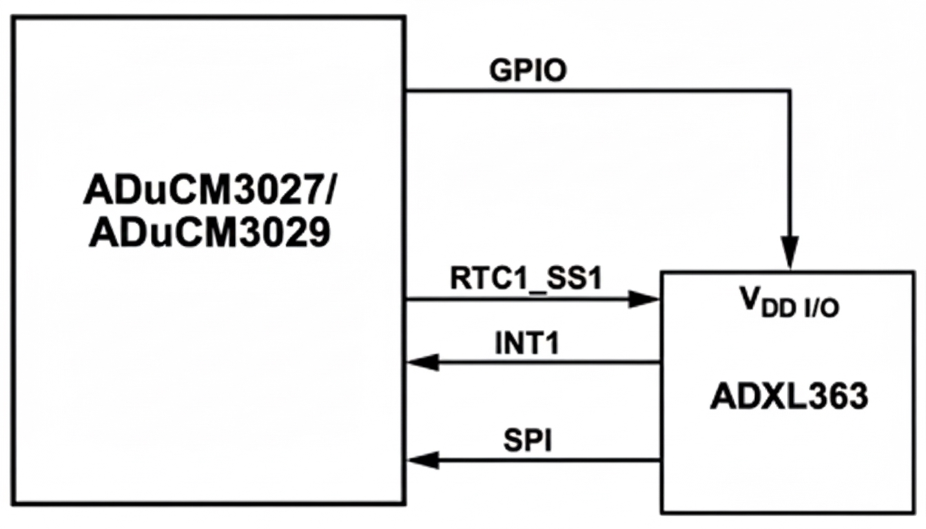
SensorStrobe is a special RTC1 alarm that produces an output pulse on the MCU's RTC1_SS1 pin. Connecting the SensorStrobe output to an external multi-sensor device such as the ADXL363 allows a low-component-count, low-power sampling solution (see Figure 7).
Analog Devices provides this subsystem as part of the ADuCM3029 EZ-KIT ADZS-UCM3029EZLITE development kit. Beyond the hardware connections, activating SensorStrobe requires only a few register writes to configure the RTC1 alarm.
While SensorStrobe runs, developers can place the ADuCM3029 in sleep mode to achieve minimal MCU consumption during extended sampling. RTC1 will count to the programmed value, then assert the SensorStrobe signal on the ADXL363 interrupt input to wake the external sensor. The sensor performs its data-sampling routine and then signals the MCU via an interrupt pin, waking the MCU to process the sampled data.
Previously, designers often used external RTCs, timers, or simple oscillators for extended sampling designs. Such external clocks increase design complexity and break time synchronization between sampled data and the MCU time base, requiring resampling or timestamp normalization. Using RTC1 with SensorStrobe ensures sampling timestamps remain synchronized to the ADuCM3029-based system.
Conclusion
The increasing demand for lower-power systems continues to challenge developers to deliver high performance in ever-smaller energy budgets. Each application requires a specific balance between functionality and power, raising development complexity.
The ADuCM3029's integrated power-management capabilities give developers flexible tools to achieve that balance. Leveraging the device's internal features simplifies implementation of application-specific tradeoffs between performance and power.