Introduction
Health is a primary concern for individuals and societies. Wearable medical monitoring systems can conveniently collect physiological data for disease prediction and early diagnosis. Wearable medical chip systems based on low-cost, low-power, and high-data-rate wireless communication technologies enable continuous acquisition of basic vital parameters during daily life. By reducing in-person clinical interactions, these systems can shorten patient wait times at clinics and help alleviate shortages in medical resources while improving the quality of care. Chronic diseases such as hypertension, diabetes, and hyperlipidemia require long-term, continuous monitoring of patients' physiological data. Wearable medical chips are small, low-power, and low-cost, making them more acceptable to patients; this potential market has attracted multiple chip design companies such as Philips, Zarlink, and TI to develop and promote related solutions.
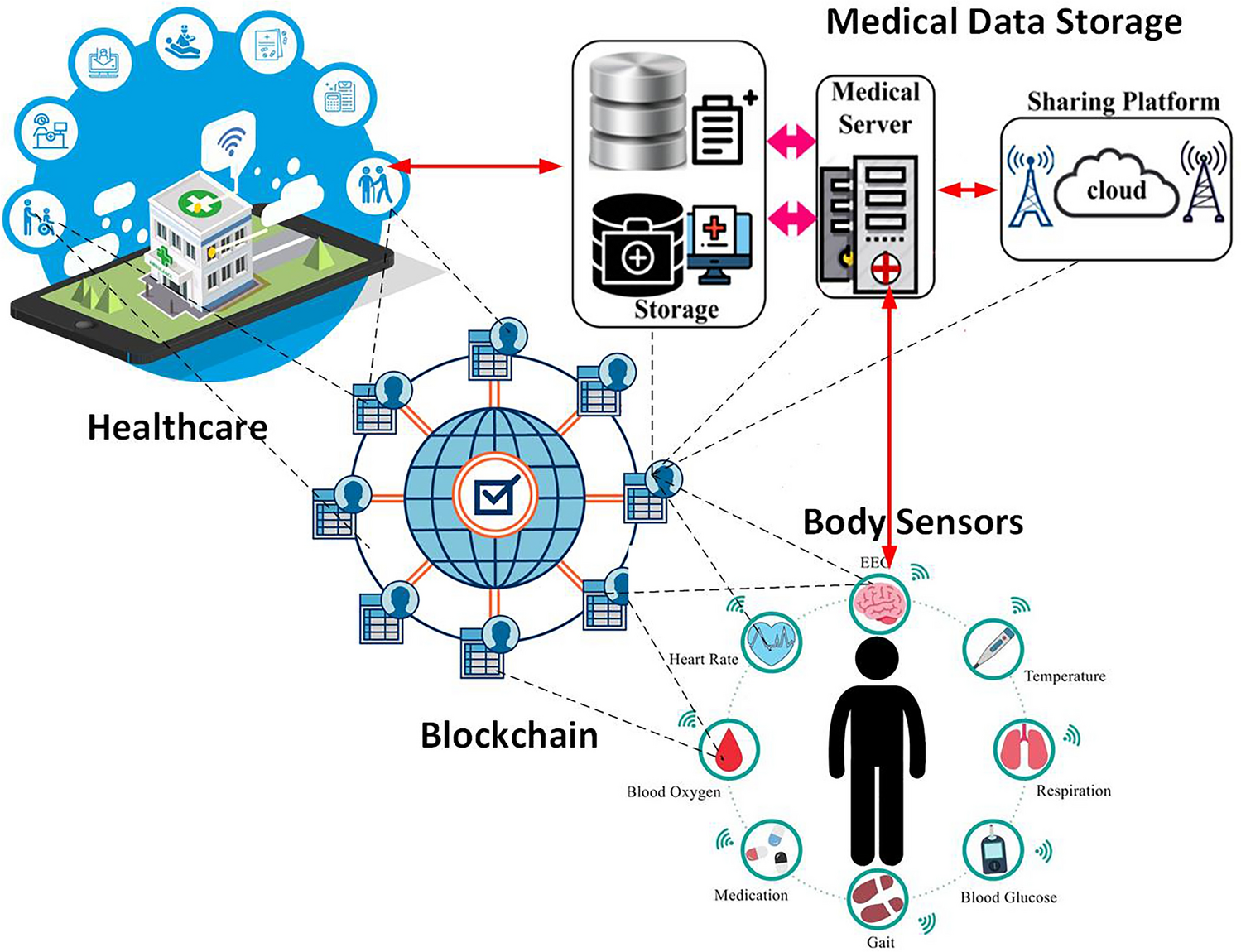
Examples of wearable sensors include fingertip blood-oxygen sensors, wrist-based glucose sensors, wrist sleep-quality monitors, sleep physiology recorders, belt-mounted respiration and heart-rate monitors, and implantable identification modules. A wireless wearable microsystem consists of distributed wireless sensors placed on the body surface, integrated into clothing, watches, or jewelry. Using wired interconnects between sensors and a central processing/display chip is inconvenient for users. Wireless communication, as a replacement for wiring, offers clear advantages. Most wireless technologies prioritize higher data rates, but wearable medical systems must also minimize power consumption during signal transmission. The transceiver block for wireless signals is often the highest power consumer on a medical chip, making low-power design of the wireless transmission circuitry a primary concern. Targeting low power and high data rate, companies such as Zarlink, Nordic, Philips, and Chipcon have introduced ultra-low-power RF transceiver solutions.
1 Wearable Medical System Chip Architecture
The overall architecture of a wearable medical chip using wireless communication typically includes physiological signal acquisition circuits, analog-to-digital converters (ADC), digital baseband processing, a controller, and RF transceiver circuitry. First, on-chip low-noise instrumentation amplifiers acquire physiological signals. These analog signals are digitized by the ADC and then processed—through encoding, FFT, and other digital-signal-processing methods—before being transmitted by the transmitter. Control signals and downlink data are received by the receiver block. The controller manages the chip operation and can be programmed to meet different application requirements. A high-performance wearable medical chip integrates high-performance digital, analog, and RF sections. The analog and RF performance directly affects overall chip performance, and they are typically the largest contributors to power consumption. Designers therefore must balance low power with adequate performance in those sections. The following subsections describe typical functional blocks of a wearable medical system chip.
1.1 Low-noise Amplifier for Physiological Signal Acquisition
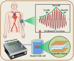
Physiological signals are usually acquired by on-chip biosensors. For integration convenience, sensors use CMOS-based low-noise amplifiers to convert biophysical signals to electrical signals. Multiple amplifier channels can be integrated to collect blood pressure, oxygen saturation, respiration rate, heart rate, body temperature, and other parameters. Because physiological signals are weak and susceptible to environmental noise, amplifiers require high sensitivity, high gain, low noise, and low power. A low-pass filter with a cutoff near 1 kHz is typically used after the amplifier to suppress out-of-band noise. Amplifiers can operate in multiple modes, such as monitor, active, and sleep, to reduce overall power consumption.
1.2 Analog-to-Digital Converter (ADC)
Multi-channel amplifier outputs are connected to the ADC input via an analog multiplexer, which selects one channel at a time. To reduce power, successive-approximation ADCs with around 10-bit resolution are common. For higher precision and throughput, sigma-delta or pipeline ADCs can be used, but they consume more power; given the critical importance of low power in wearable designs, trade-offs are necessary. The unit capacitance in charge-based ADCs should be chosen carefully: larger capacitances occupy more die area and increase susceptibility to parasitics.
1.3 Controller
The controller may be an ARM core or an MCU that controls operating modes across chip blocks, manages data timing, configures registers, and coordinates on-chip communications.
1.4 Digital Baseband Signal Processing
To improve data throughput, reliability, and security, ADC outputs are processed by a digital baseband processor for compression, encoding, FFT, and digital filtering to further remove interference.
1.5 RF Transceiver
Because wearable sensors are placed at different body locations, wired interconnects are inconvenient and prone to tangling. Wireless transmission is the natural alternative. The design considerations for an integrated RF transceiver in wearable medical chips differ from those of typical wireless products. Wearable systems often have asymmetric traffic: uplink telemetry from sensors dominates, while downlink control commands are sparse. This allows half-duplex operation with low-rate downlink and higher-rate uplink. Wearable devices must operate for long periods on small batteries such as coin cells with 1.2–1.5 V nominal voltage and limited capacity. The RF transceiver is often the largest power consumer, so designers face the challenge of achieving low supply voltage, low power, and adequate data rates. Key design decisions include architecture, carrier frequency, modulation scheme, data rate, and power consumption.
2 Wireless Communication Standards for Wearable Medical Chips
Wireless communication standards evolve rapidly and have significantly influenced modern medical technology. Multiple standards can serve wearable medical chip applications; each standard suits specific use cases but may not fully exploit the low-power, short-range characteristics of wearable medical devices. The following summarizes the features and trade-offs of common standards.
2.1 Bluetooth
Bluetooth uses frequency-hopping and spread-spectrum techniques to suppress intersymbol interference and maintain link quality. It supports ranges approximately 1, 10, and 100 meters and data rates up to 1 Mbps. It offers simple architecture and low component cost. Bluetooth supports point-to-point serial communication and shared-channel master-controller interfaces, making it suitable for personal area networks. However, Bluetooth operates at 2.4 GHz, which is a relatively high frequency for close-body operation and typically consumes more power than some alternative technologies, making it a less-than-ideal choice for ultra-low-power wearable medical applications.
2.2 Zigbee
Zigbee operates in 2.4 GHz, 900 MHz, and 800 MHz bands. Compared with Bluetooth, Zigbee can offer lower power consumption. At 2.4 GHz, its maximum data rate is 240 kbps. Drawbacks include relatively low throughput, higher latency, weaker security compared with some alternatives, and susceptibility to interference in the crowded 2.4 GHz band.
2.3 UWB
Ultra-wideband (UWB) spans roughly 3.1–10 GHz and can provide average data rates near 850 kbps up to tens of Mbps. The standard specifies low power spectral density, allowing pulse-based transmission with simple transmitters and placing more design complexity in the receiver. Since wearable telemetry is typically uplink-heavy, UWB suits asymmetric communication, reducing system complexity and potentially lowering power.
2.4 WLAN 802.11
IEEE 802.11 WLAN operates in ISM bands. Variants such as 802.11b/g at 2.4 GHz and 802.11a at 5 GHz provide high throughput (11–54 Mbps) and good interference resilience via direct-sequence spread spectrum. However, WLAN systems are power-hungry, complex, and relatively expensive, making them unsuitable for most wearable medical chip designs.
2.5 Wireless USB
Wireless USB, like UWB, uses ultra-wideband techniques in 3.1–10.6 GHz and supports short-range high-speed links, with data rates up to hundreds of Mbps. Its main challenge for wearable use is power consumption.
2.6 Infrared Communication (IrDA)
Infrared offers low cost and simple implementation but requires line-of-sight, is limited to short-range point-to-point links with alignment, and has modest data rates, making it inconvenient compared with other wireless options.
2.7 RFID
RFID uses electromagnetic coupling to enable contactless data exchange. Frequency allocations vary by region; for example, China's planned RFID bands include 50–190 kHz, 13.56 MHz ±7 kHz, 432–434.79 MHz, and specific UHF points near 900 MHz used in vehicle identification. RFID is suitable for short-range, indoor applications such as asset tracking, inventory, patient monitoring, and drug tracking. However, RFID offers low data rates and limited security, so it is generally not appropriate for real-time wearable medical telemetry.
2.8 Body Communication
Body communication, or bio-channel communication, is a more recent concept that uses the near-body magnetic field or the body itself as the communication medium. Proposed first by Zimmerman at the MIT Media Lab in 1995, this approach supports very short-range links, sometimes requiring contact, which enables precise control of communication range and endpoints and reduces cross-channel interference while improving security. Compared with wired near-body links that ensure high-speed, accurate transmission but suffer from tangling, and with general-purpose wireless technologies such as Zigbee and Bluetooth that can be slower and more power-consuming, body communication offers attractive trade-offs for wearable systems.
3 Examples of RF Transceiver Development for Wearable Medical Chips
Advances in microelectronics and the growing need for continuous health monitoring have driven development of wearable medical systems. A body area network (BAN) comprises many sensor nodes; each node communicates with others or a central node using an on-chip RF transceiver. Early short-range medical telemetry chips used ASK/FSK modulation with low-power crystal oscillators, which only supported single vital-sign transmission, had long oscillator startup times, and low data rates. Inductive coil-based solutions were also proposed but suffered from poor link quality and low throughput.
Nonstandard systems could not meet requirements for ultra-low power, tiny size, reliability, and sufficient data rate. Driven by growing demand, research institutions and chip companies developed targeted solutions, including Zarlink's ZL70101 RF transceiver, Toumaz's Sensium SoC, low-voltage low-power 2.4 GHz transceivers from academic groups, and body-communication transceivers developed by research institutes.
3.1 Zarlink Implantable Communication System: ZL70101
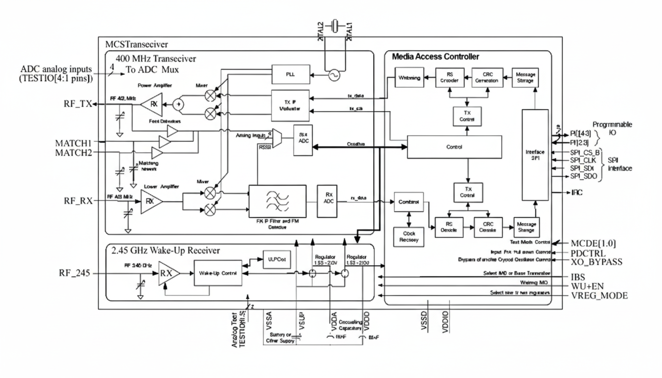
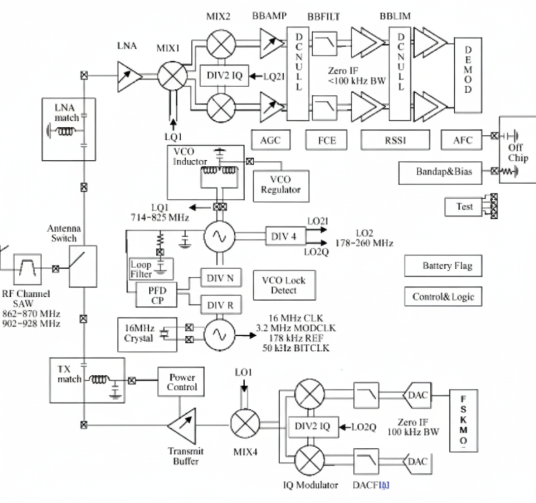
In 2006, Zarlink Semiconductor released the ZL70101, an ultra-low-power RF transceiver for implantable medical systems. The device integrates highly and requires only a 24 MHz quartz crystal and two decoupling capacitors as external components, excluding matching networks. It operates in the 433 MHz ISM band using a 0.18 μm RF CMOS process. The transceiver consumes 5.5 mA in active receive operation and just 250 nA in sleep mode. The chip integrates a 400 MHz RF transceiver, a 2.45 GHz wake-up receiver, and a MAC controller.
The receiver uses a low-IF architecture with a low-noise amplifier, image-reject mixer, IF image-suppression multiphase filter (PPF), received signal strength indicator (RSSI), and ADC. The transmitter comprises an upconverter and a power amplifier using FSK modulation. The wake-up system is an OOK receiver at 2.45 GHz that periodically listens for base-station wake-up signals to turn on the main chip power, greatly reducing average current consumption. Although designed for implantable applications, the ZL70101's ultra-low power, 2 m range, and up to 800 kbps data rate also suit external wearable device interconnection.
3.2 Toumaz Sensium Ultra-Low-Power SoC Transceiver
In 2007, Toumaz released the Sensium system-on-chip, integrating SPI, ADC, MCU, RAM, and an ultra-low-power RF transceiver. The transceiver area is about 7 mm2 in a 0.13 μm RF CMOS process, operating from a 1 V supply and supporting European 870 MHz and U.S. 928 MHz bands. Receive current is about 2.1 mA and transmit current about 2.6 mA at a transmit power around -7 dBm. The transceiver uses half-duplex FSK with 50 kbps data rate and a BER around 10^-3. It targets ECG, cardiac pacing, and body-temperature telemetry. A sliding-IF architecture provides improved image rejection compared with low-IF designs and reduced DC offset compared with zero-IF receivers.
To meet low-power requirements, the SoC runs at 1 V, below the sum of PMOS and NMOS threshold voltages in 0.13 μm, so many analog and RF transistors operate in subthreshold or weak-inversion regions to save power, which complicates analog/RF design. The receiver uses a zero-IF architecture in parts, and the LNA is a single-ended source-gate configuration with on-chip planar inductors and a tunable capacitor matrix for matching. The mixer uses a Gilbert-cell double-balanced topology in a pseudo-differential mode. The final transmit driver is an open-drain single-NMOS stage directly connected to an off-chip LC matching network; this stage requires a thick-oxide dual-gate NMOS to prevent gate oxide breakdown. The transmitter uses a simple VCO in self-oscillating mode. Link loss is compensated with RSSI-based AGC, and the transmit driver gain is adjustable to improve power-efficiency.
3.3 Body-Communication RF Transceiver Chip
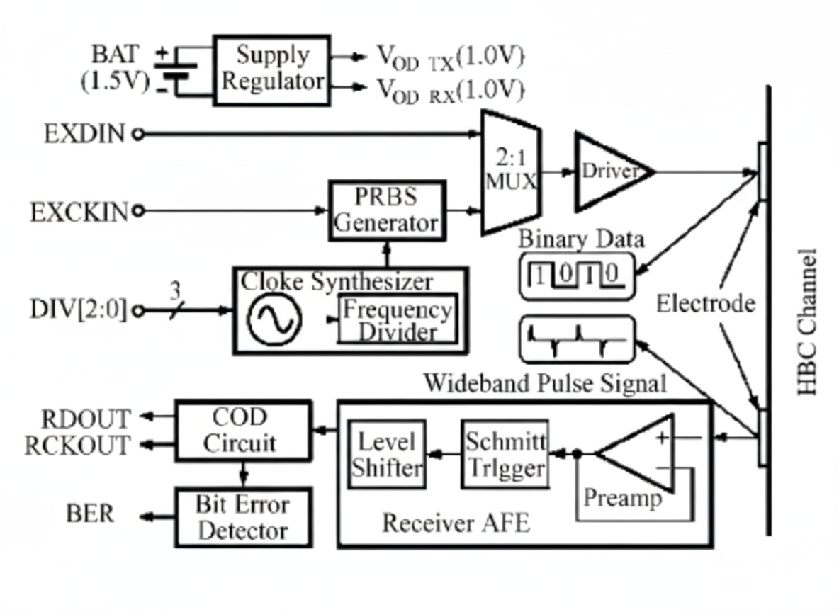
In 2007, a research group led by Seong-Jun Son at the Korean Academy of Sciences designed an extremely low-power body-communication transceiver achieving up to 2 Mbps. The chip uses wideband techniques similar to UWB and transmits data via near-body magnetic-field conduction. The fully digital transceiver operates from a 1 V supply with power consumption around 0.2 mW and a die area of 0.85 mm2, making it suitable for short-range, high-data-rate, ultra-low-power wearable interconnects.
The design supports operating frequencies from 1 to 200 MHz using a 0.25 μm CMOS process. Only a single signal electrode contacts the skin or clothing, eliminating the need for a separate global ground electrode. The transmitter includes a ring oscillator, a pseudo-random binary sequence (PRBS) generator, and a driver buffer. The receiver comprises an analog front end amplifier, level-shifting circuitry, a Schmitt trigger, and a clock-data recovery PLL. To reduce power, the chip uses unmodulated direct digital transmission, 200 MHz wideband signaling, fully digital clock recovery, digitally controlled oscillators (DCO), and quadrature sampling techniques. These low-power circuit techniques minimize consumption in the front-end amplifier and clocking circuits.
4 Outlook for Wearable Medical RF Transceiver Chips
With increasing life pressures and higher personal health expectations, wearable medical chips are gradually entering everyday use. As biomedical engineering and microelectronics evolve, wearable devices are trending toward miniaturization and networking. Wearable microsystems require sensor nodes to be compact and comfortable for long-term wear while enabling wireless transmission of physiological data to central stations or other sensor nodes, making networked operation a fundamental requirement. Consequently, future wearable medical chips will move toward full-system SoC integration to achieve miniaturization and lower cost, with on-chip RF transceivers enabling convenient, real-time sensor data transmission for continuous health monitoring.
There is not yet a single dedicated international wireless standard for personal wearable medical systems; instead, IEEE 802.15 family standards for low-cost, low-power wireless are commonly adopted. Although some wearable medical chips based on Zigbee, Bluetooth, and WLAN exist, those protocols were not specifically designed for wearable medical applications, and their MAC and QoS layers cannot be optimally tuned for the low-power, short-range, high-rate needs of wearable telemetry. Designers therefore have significant opportunities to innovate in low-power circuit techniques and wireless transmission methods. With ongoing advances in wireless communications, integrated-circuit technology, and market development, these challenges are expected to be addressed, guiding medical wearable engineering toward lower cost, smaller size, greater intelligence, and improved connectivity.