Overview
Recently, Samsung announced plans to produce a ninth-generation V-NAND next year, reportedly using a dual-stack architecture and exceeding 300 layers. In August, SK Hynix said it will further refine a 321-layer NAND flash and plans volume production in the first half of 2025. Earlier in May, eeNews Europe reported that engineers at Western Digital and Kioxia were working on eight-plane 3D NAND devices and 3D NAND ICs with more than 300 word lines.
01 Layer Count “Race”
Although solid-state drives (SSDs) deliver high transfer speeds, cost and capacity remain challenges. The 2.5-inch form factor limits space for memory chips; higher-capacity chips increase overall drive capacity but also raise cost and retail price.
Intel and Micron developed 3D NAND as a way to overcome the scaling limits of planar NAND. 3D NAND stacks memory cells vertically to avoid the physical limitations of two-dimensional designs. Planar NAND was nearing its practical scaling limit, creating pressure on the semiconductor memory industry. By vertically stacking multiple layers of storage cells, 3D NAND achieves much higher density and can deliver up to several times the capacity of comparable planar NAND. This enables higher capacity in a smaller footprint, reducing cost per bit, lowering power consumption, and improving performance to meet the needs of consumer mobile devices and enterprise deployments.
In 2007 Toshiba first proposed the 3D NAND structural concept. Samsung introduced its V-NAND (3D NAND) in 2013. The 3D design introduced alternating layers of polysilicon and silicon dioxide and replaced floating-gate cells with charge trap flash (CTF). Unlike floating-gate architectures that store charge in a conductive layer, CTF traps charge in a dielectric layer. This 3D approach improved performance and helped control cost.
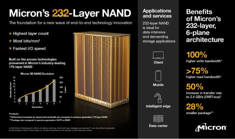
Samsung continued to update its technology and expand production lines, releasing multiple generations over a decade. In 2020 Samsung introduced the seventh-generation V-NAND with 176 layers using a double-stack process, where layers are produced in two parts and then stacked. In late 2022 Micron announced it would begin volume production of a next-generation 232-layer 3D NAND by the end of the year, signaling continued development beyond 176-layer technology toward higher-layer architectures. Micron's 232-layer 3D NAND was used in several Crucial SSDs and aimed to deliver greater capacity, higher density, lower energy per bit, and reduced cost per unit of storage.
With the rise of big data and cloud computing, demand for NAND Flash continues to grow, driving ongoing NAND technology upgrades and intensified competition over layer counts among NAND manufacturers.
02 Differences Among 300+ Layer Approaches
SK Hynix is the first company to disclose development of a NAND flash above 300 layers, announcing a 321-layer 4D NAND sample on August 9. This is SK Hynix's eighth-generation 3D NAND, with a capacity of 1 Tb (128 GB), triple-level cell (TLC) configuration, and bit density above 20 Gb/mm2. The chip has a 16 KB page size, four planes, an interface transfer rate of 2400 MT/s, and a peak throughput of 194 MB/s, an 18% improvement over the previous seventh-generation 238-layer 3D NAND. Increased density reduces manufacturing cost per terabit, benefiting end users through improved performance and capacity.
SK Hynix cites five key technologies in its eighth-generation 3D NAND: triple-verify programming (TPGM) to narrow threshold-voltage distribution and reduce tPROG by about 10% to improve performance; adaptive unselected-string precharge (AUSP) to lower tPROG by roughly 2%; programming virtual strings (PDS) to reduce channel capacitance load and shorten tPROG and tR worldline setup time; plane-level read retry (PLRR) to change read levels on one plane without terminating others to immediately issue follow-up read commands and thus improve QoS and read performance; and other optimizations. SK Hynix plans to use a triple-stack technique, producing three independent 3D NAND stacks of 120, 110, and 91 layers respectively, then combining them into a single chip, with volume production expected in 2025.
Samsung, however, aims to beat SK Hynix to volume production. Korean media Seoul Economic Daily, citing industry sources, reported Samsung plans to produce 300+ layer ninth-generation 3D NAND in 2024 using a dual-stack process that creates NAND stacks in two separate processes and then integrates them. This approach differs from SK Hynix's triple-stack method. Samsung began volume production of eighth-generation V-NAND at the end of 2022, delivering a 236-layer 1 Tb TLC 3D NAND chip that used a dual-stack approach, a major increase from the 176-layer seventh-generation V-NAND introduced in 2020. Samsung's roadmap indicates NAND stacking could exceed 1,000 layers by 2030.
Kioxia and Western Digital reported innovations enabling higher-capacity, higher-performance 3D NAND devices. According to eeNews Europe, engineers from both companies are pursuing eight-plane 3D NAND devices and 3D NAND ICs with more than 300 word lines. Kioxia presented an eight-plane 1 Tb 3D TLC NAND die with over 210 active layers and a 3.2 GT/s interface. Kioxia's data show program throughput of 205 MB/s and latency around 40 microseconds.
The eight-plane 1 Tb 3D TLC die reduces the X-direction data query region to 41% to achieve the 3.2 GT/s interface rate, which could cause routing congestion. Kioxia mitigated this through a hybrid row-address decoder to minimize latency degradation from congestion. Kioxia also introduced a single-pulse dual-select sensing technique that senses two storage cells within one pulse, reducing total sensing time by 18% and boosting program throughput to 205 MB/s.
These two innovations deliver higher performance and lower latency, but an eight-plane architecture increases IC and controller complexity, raising development and manufacturing cost. If a controller cannot properly manage eight-plane dies, actual IC performance may degrade. In addition to eight-plane 3D NAND ICs, Kioxia and Western Digital jointly developed 3D NAND dies exceeding 300 layers. Their joint teams used metal-induced lateral crystallization (MLIC) to form single-crystal silicon channels approximately 14 micrometers long inside vertical storage holes, and applied advanced nickel-gettering techniques to remove silicon impurities and defects. These measures reduced read noise by at least 40% and increased conductance by 10 times.
03 Strategic Importance of High-Capacity Storage
Market dynamics, demand, and technology continue to change, and storage market volatility affects the broader semiconductor industry. In 2023 NAND suppliers acted to rebalance supply and demand by cutting shipments and reducing fab utilization. Market research firm Yole reported that suppliers reduced 2023 capital expenditures and delayed roadmap progress, with NAND capex expected to decline about 40% year over year. Yole noted that normalization of inventories and restored OEM procurement confidence could support a NAND recovery later in the year.
Yole Intelligence's recent report indicated the NAND Flash market would return to growth in the third quarter, ending nearly two years of decline. Global demand for data generation and storage continues to grow, and the adoption of new technologies supports a positive long-term outlook for NAND Flash. Factors cited include increased enterprise SSD demand from hyperscalers and OEMs for large-scale data processing; wider SSD adoption in PCs and game consoles for faster boot and higher I/O performance; and growing storage needs in smartphones and other mobile devices as users store more photos, videos, and apps. These trends are expected to drive NAND Flash market growth.
Analysts predict the NAND market will end seven consecutive quarters of decline and return to growth in the third quarter.