Introduction
In recent years artificial intelligence applications have seen rapid development and wider deployment, with large models such as ChatGPT playing a key role. These models drive continuously increasing demands for computation, leading to major innovations in AI chip design and a shift into a high-compute era.
Most mainstream AI chips still use the traditional von Neumann architecture, which separates compute units from data storage. In this model, processors read data from memory, perform computations, and write results back to memory. Even though peak compute capacity has increased substantially, raw compute performance alone is insufficient: when data transfer cannot keep up with computation, memory transfer time can dominate overall execution time.
Transformer-based large models have caused parameter counts to balloon: model size increased dramatically over a short period, and compute requirements rose even more steeply. While peak hardware compute improved by orders of magnitude over the past two decades, DRAM bandwidth growth has lagged behind. This gap between compute and bandwidth creates a bottleneck in memory capacity and data transfer speed, commonly referred to as the "memory wall."
Responses to the Memory Wall
Researchers and developers are pursuing multiple approaches to mitigate the memory wall. The main directions are:
- Algorithm optimization: Revisit network model designs and optimize algorithm implementations to reduce dependence on high-speed data transfers. The goal is to lower data movement requirements and improve algorithmic efficiency.
- Model compression: Reduce model size through lower precision (quantization) or removal of redundant parameters (pruning). This reduces memory footprint and eases pressure on the memory subsystem.
- AI chip architecture design: Design chip architectures that optimize data flow and computation. Hardware-level innovations aim to reduce data movement and computation overhead, improving overall system efficiency.
Algorithm optimization and model compression are major focuses for software teams. In hardware, AI chip vendors are also optimizing architectures to improve memory transfer efficiency. One such example is Ambarella's CV3 series and its CVflow architecture.
How the CV3 Series Addresses the Memory Wall
Ambarella began exploring automotive chip requirements after acquiring the autonomous driving algorithm company VisLab in 2015. The company introduced the first CVflow-based chip, CV1, in 2017 to accelerate AI vision processing, and then the CV2 series for automotive advanced driver assistance systems (ADAS) starting in 2018. As autonomous driving demands increased, Ambarella initiated CV3 design work to provide higher compute for driving scenarios. In 2022 the first CV3 architecture chip, CV3-HD, was powered on with up to 1500 eTOPS (equivalent) at about 50 W. In 2023 the CV3-AD685, aimed at production AD domains, reached 750 eTOPS and entered sampling. In January 2024 Ambarella introduced additional CV3-AD members, CV3-AD635 and CV3-AD655, extending the CV3-AD series coverage across mainstream to higher-end passenger vehicle ADAS and autonomous driving use cases.
To address memory bandwidth challenges, CV3 uses an advanced LPDDR5 memory controller, with DRAM data rates up to 8 Gb/s per DRAM lane. The design offers 64-, 128-, and 256-bit memory widths to match different application bandwidth needs.
CVflow Architecture Overview
The CV3 family adopts Ambarella's third-generation CVflow architecture for its AI accelerator. CVflow structures data flow and compute units to improve compute efficiency and energy efficiency. The overall architecture and data organization are illustrated below.
CV3's high compute and low power characteristics arise from several architectural choices described below.
Partial buffer architecture
Many AI chips increase on-chip cache to reduce DRAM accesses, but large cache systems present several challenges:
- Design complexity and cost: Cache systems are complex and occupy more chip area than equivalent SRAM, increasing cost and possibly power.
- Software optimization requirements: Achieving high cache hit rates requires software changes and optimizations, increasing development complexity.
- Compute underutilization: Caches often use a load-on-demand model, so compute units may idle while waiting for data loads, making compute utilization dependent on cache hit rates.
- Performance variability: Cache hit rates depend on system load and can vary in multi-core, multi-threaded environments, causing unstable performance.
CVflow takes a different approach by partitioning on-chip memory into multiple blocks of different sizes called Partial Buffers (PB). PBs store intermediate computation results and greatly reduce external DRAM accesses. The Partial Buffer approach provides several advantages:
- Simplified hardware and lower cost: PBs are simpler than full caches, saving chip area and reducing manufacturing cost and power.
- Dedicated DMA channels: PBs are served by independent DMA (Direct Memory Access) channels, enabling fast, seamless transfers from DRAM into PBs and avoiding transfer bottlenecks.
- High memory access efficiency: Transferring large contiguous data blocks between DRAM and PBs in single operations reduces the number of data moves between memory and the vector processor (NVP), lowering latency and overhead.
- Parallelism with compute units: PBs are organized in a ring structure inside CVflow. When one PB's data is consumed, the hardware scheduler loads the next required block into a free PB. This enables data preloading in parallel with computation and removes data-wait stalls.
- Simplified memory management: CVflow tooling automatically and efficiently manages PBs, reducing developer effort on on-chip memory management.
For example, a convolutional neural network that would require 12 DRAM accesses in a conventional architecture can, under CVflow, replace many of those accesses with low-latency PB operations. Intermediate results remain in PBs and do not require repeated external DRAM accesses. Typically only one DRAM access at input and one at output are needed, reducing DRAM accesses by up to 10 times, lowering latency and overall power.
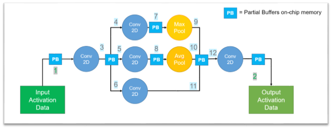
Figure 1 CVflow convolution example
Parallel streaming architecture
CVflow tooling partitions large neural networks into a sequence of compact compute units organized as a directed acyclic graph (DAG) according to available on-chip memory. This approach yields multiple benefits:
- Efficient memory utilization: Intermediate computations for each DAG segment are completed on-chip, avoiding frequent external DRAM access and reducing data transfer latency.
- Fast startup and parallel loading: The system can begin computation with only a portion of the network loaded. CVflow loads subsequent network segments in parallel with ongoing computation, improving end-to-end throughput.
- Stable performance under mixed load: By greatly reducing DRAM accesses and enabling compute-data parallelism, CVflow maintains stable performance even when other chip modules (CPU, GPU, ISP) experience high load.
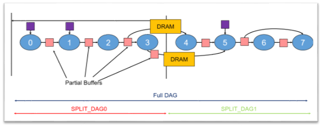
Figure 2 DAG partitioning for AI models
Hardware operator implementation
Unlike GPUs that scale compute by adding general-purpose compute units, CVflow emphasizes efficient hardware operators. Based on forward-looking study of deep learning networks, CV3 implements hardware versions of over 100 common operators. This allows CVflow to deliver strong compute using fewer transistors.
For example, an 8x8 matrix multiply traditionally requires 512 multiply-accumulate (MAC) operations, but CVflow's dedicated matrix multiply operator can complete the operation within a single compute instruction cycle. CVflow also supports fused operators: common sequences like convolution plus pooling can be fused into a single hardware operator by the CVflow tooling, reducing data movement and compute cycles.
Unstructured sparsity acceleration
Sparsifying models to remove redundant parameters yields notable performance improvements under CVflow:
- CVflow tooling can automatically compress network parameters, reducing the time to load models on the chip.
- The CVflow hardware scheduler can detect and skip unnecessary computations, lowering overall compute work.
- No structural changes to model topology are required, enabling one-time algorithm development and seamless deployment without compatibility concerns.
- The toolchain offers multiple sparsity strategies to preserve model accuracy after sparsification.
For instance, a 7x7 convolution uses 49 parameters and 49 MAC operations per output location. After 80% sparsification, parameter storage and transmission requirements drop substantially and compute decreases by about 80%, greatly improving convolution efficiency. CVflow's sparsity techniques are important for optimizing model performance and resource use.
Support for multiple quantization formats
CVflow supports fixed-point formats of 4, 8, 16, and 32 bits and floating-point formats of 16 and 32 bits. The tooling performs per-layer dynamic range analysis for parameters and I/O to determine optimal quantization precision and enable efficient mixed-precision deployment. This flexibility helps CV3 adapt to different data types and task scales.
Practical validation and outlook
At CES 2024 Ambarella demonstrated an autonomous research vehicle based on the CV3 platform. The demonstration provided practical validation that the CV3 CVflow architecture can handle the high compute and bandwidth demands of automotive driving scenarios.
With the trend toward end-to-end large-model autonomous driving, the compute and memory wall challenges will grow. CV3-AD series chips, designed for automotive domains and based on the third-generation CVflow architecture, address the memory wall through architectural innovations. These chips provide hardware support for large-model algorithms used in advanced driver assistance and autonomous driving development.