Introduction
In FPGA design, BRAM is a key on-chip memory resource. FPGA development requires familiarity with BRAM. This article reviews BRAM concepts, composition, and common applications.
1. BRAM overview
Definition
RAM stands for Random Access Memory, a memory where data is accessed by addressable memory cells. BRAM, or block RAM, refers to dedicated RAM resources placed at fixed locations inside the FPGA. Distributed RAM is implemented using LUT logic resources inside the FPGA.
BRAM components
In Xilinx FPGAs, the physical BRAM resources correspond to RAMB36E1 and RAMB18E1 blocks.
RAMB36E1
RAMB36E1 is a 36 KB block RAM, internally composed of two independent 18 KB block RAMs (RAMB18E1). A 36 KB block memory can be configured in four ways:
- As a single 36 KB BRAM;
- As a single 36 KB FIFO;
- As two 18 KB BRAMs;
- As one 18 KB BRAM and one 18 KB FIFO.
Note that it cannot be configured as two separate 18 KB FIFOs because the block memory includes a single FIFO control logic structure used to generate FIFO control signals (including read/write addresses). Since this control logic is unique and not shareable, at most one FIFO can be instantiated per block memory.
RAMB18E1
RAMB18E1 is an 18 KB block RAM and is a primary built-in block RAM primitive in Xilinx FPGAs, providing high-speed synchronous memory access.
BRAM quantity in FPGAs
The number of BRAM blocks varies by FPGA model. For example, Xilinx Kintex-7 series devices provide different counts of BRAM resources depending on the specific part.
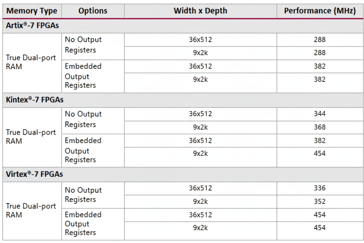
BRAM performance
Whether an FPGA embeds output registers in BRAM affects the maximum operating clock frequency of the BRAM. Different FPGA models offer different BRAM timing characteristics and performance capabilities.
2. BRAM applications
ROM
BRAM can be used as ROM by initializing contents at IP definition or instantiation time. A ROM configuration supports read-only access.
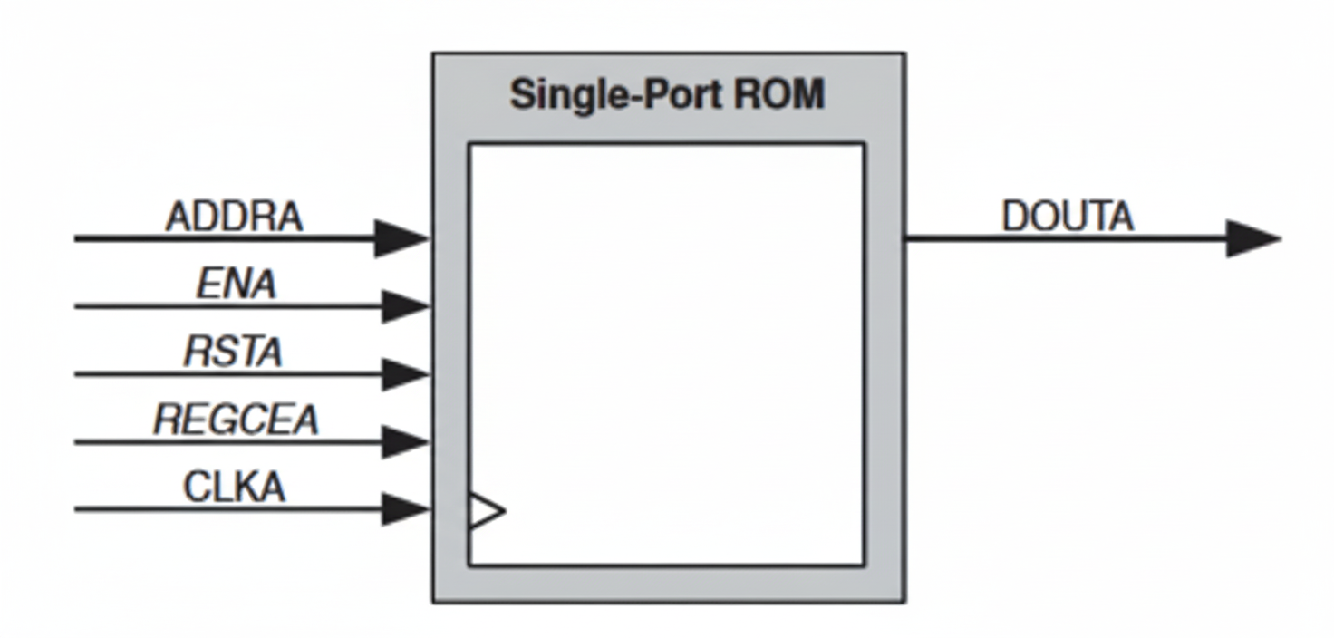
Single-port ROM
A single-port ROM provides one read port and is suitable for storing program code or initialization tables.
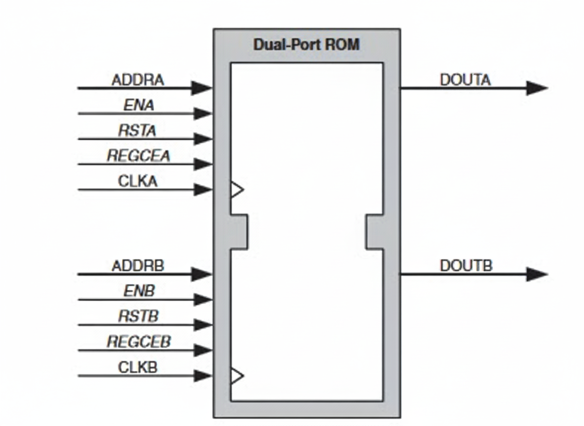
Dual-port ROM
A dual-port ROM provides two independent read data ports and is useful for sharing the same ROM between two processors or systems.
RAM
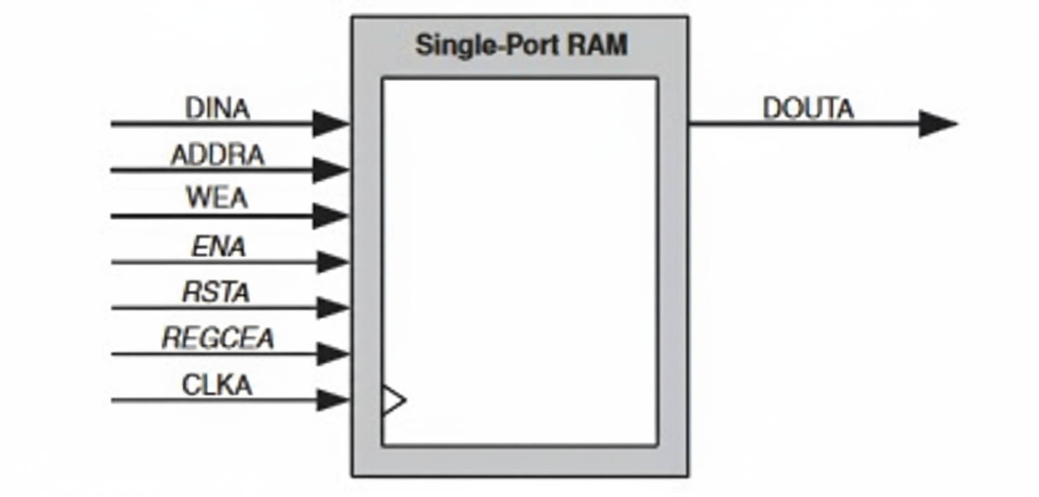
Single-port RAM
Single-port RAM exposes one port that can be used for either read or write access.
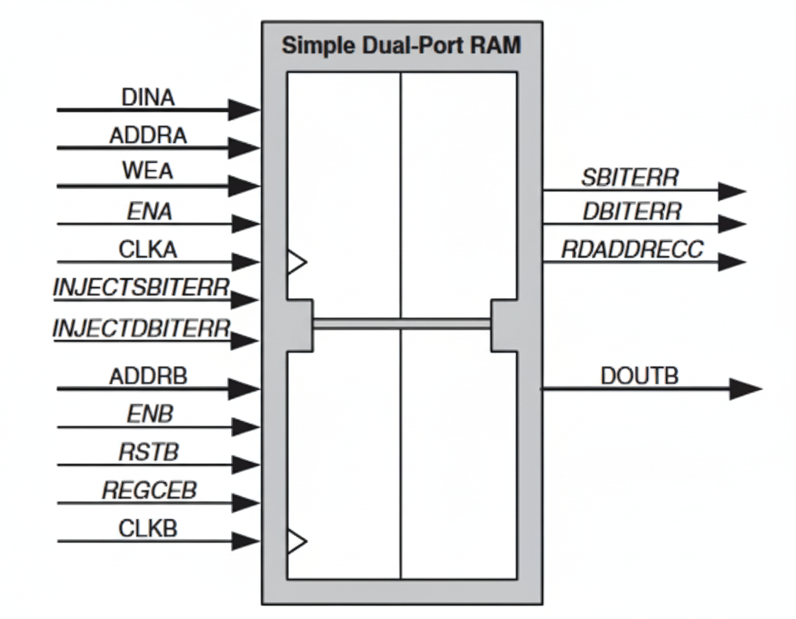
Simple dual-port RAM
Simple dual-port RAM has two ports, A and B. Port A typically supports write while port B supports read.
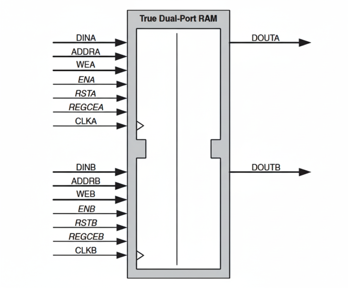
True dual-port RAM
True dual-port RAM provides two ports, A and B, and each port can independently perform read and write operations.
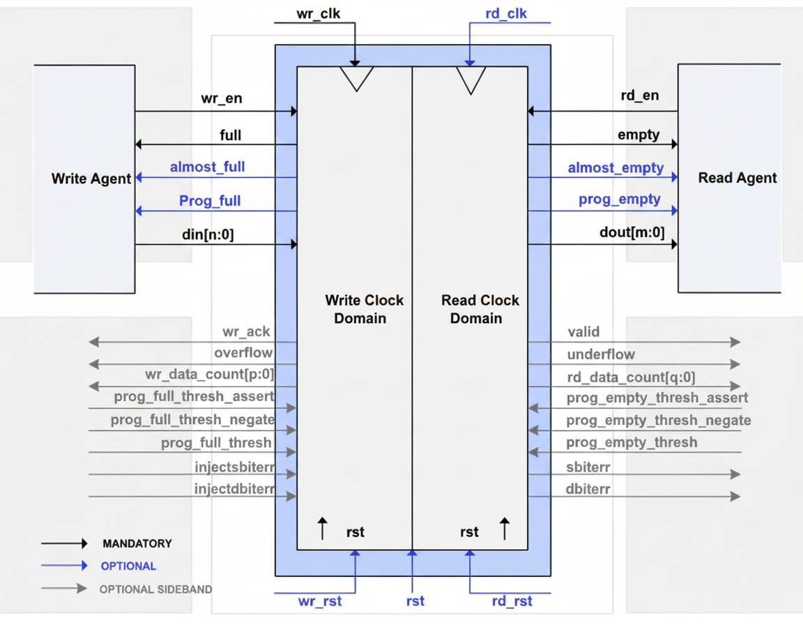
FIFO
FIFOs can be implemented using BRAM to provide first-in-first-out buffering. There are synchronous FIFOs and asynchronous FIFOs depending on whether read and write sides share the same clock domain.
Summary
BRAM is a dedicated on-chip memory resource in FPGAs with excellent performance but limited quantity. A typical BRAM block is 36 KB in size and can be configured as two 18 KB blocks. BRAM can implement various memory structures with different data widths and depths, such as RAM, ROM, and FIFO, and is widely used and flexible within FPGA designs. Proper use of BRAM enables high-speed buffering, pipelining, and other on-chip memory optimizations in FPGA projects.