Overview
The primary development directions for DDR memory are higher transfer rates, lower operating voltages, and greater storage density to achieve improved performance.
DDR4 SDRAM (Double Data Rate fourth-generation SDRAM): DDR4 uses a lower supply voltage of 1.2 V and offers higher bandwidth than DDR3 and DDR2. Transfer rates currently range from about 2133 to 3200 MT/s. DDR4 introduces a Bank Group design with four bank groups, each capable of independently issuing activate, read, and write operations. The bank-group concept allows DDR4 to handle multiple transactions within the same operating cycle, increasing effective throughput compared with DDR3. DDR4 also adds features such as DBI (Data Bus Inversion), CRC (Cyclic Redundancy Check), and CA parity to improve signal integrity and data reliability while operating at higher speeds and lower power.
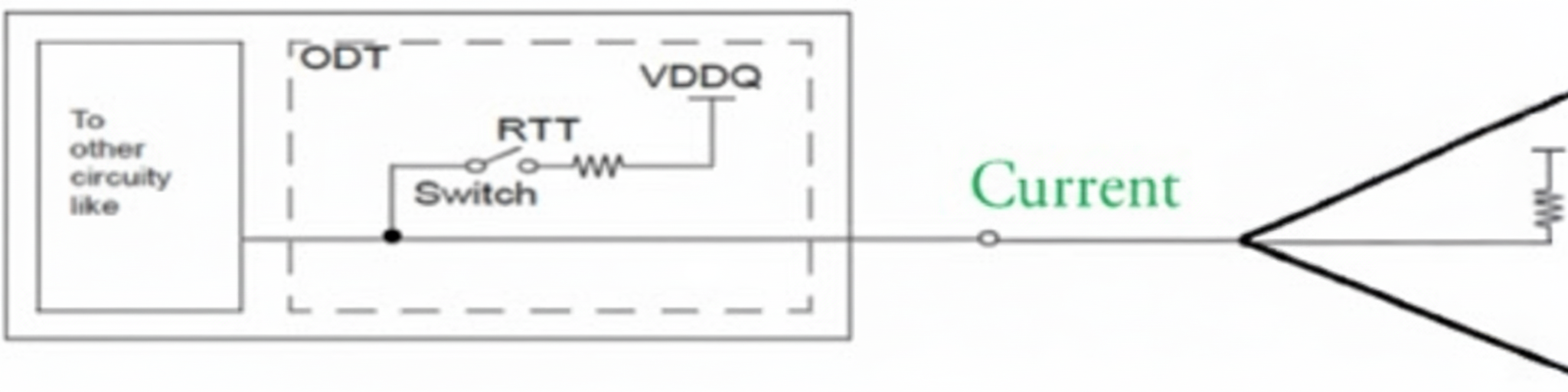
POD and SSTL Comparison
POD is a new driver/termination standard used in DDR4. The key difference is that the POD receiver termination voltage equals VDDQ, while DDR3 uses an SSTL termination voltage of VDDQ/2. This reduces parasitic pin capacitance and I/O termination power and allows stable operation even when VDD is reduced. The equivalent circuits are shown below for DDR4 (POD) and DDR3 (SSTL).
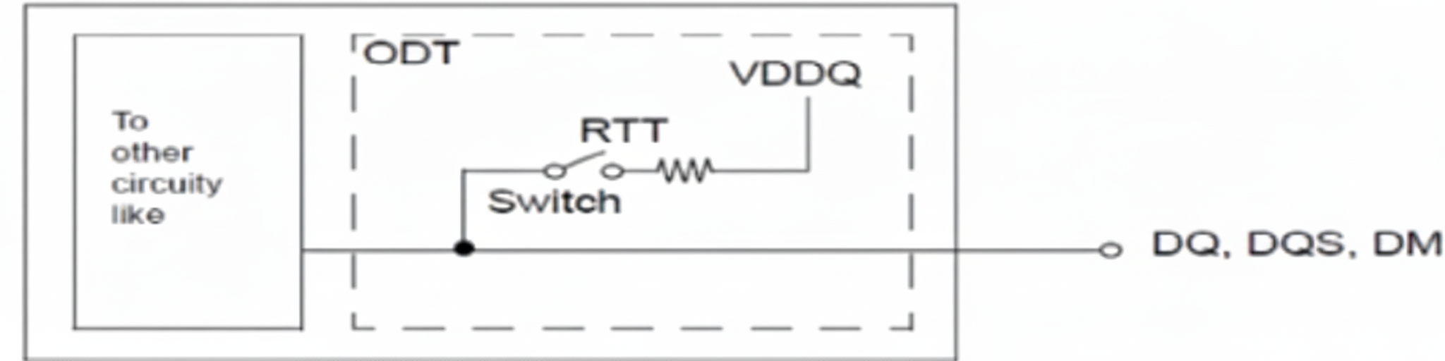
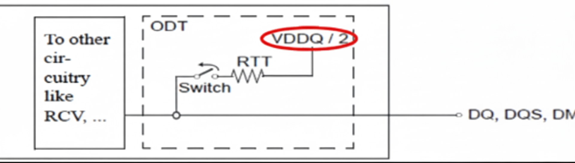
When DRAM is at a low logic level, both SSTL and POD have current flow. When DRAM is at a high logic level, SSTL still has current flow while POD does not, because the termination ends are at equal voltage. This absence of current in the high state is one of the reasons DDR4 reduces power consumption.
Bank Group (BG) Design
A standards organization determined that increasing data prefetch depth had become more difficult to scale, so the Bank Group architecture was introduced. Each bank group can independently perform activate, read, write, and refresh operations, which significantly increases internal data throughput and effective memory frequency.
DDR4 uses an 8n prefetch tied to bank-group partitioning. Systems may use two or four selectable bank groups. With two independent bank groups, the effective prefetch becomes 16n; with four independent bank groups, the effective prefetch becomes 32n. This approach improves overall memory efficiency and bandwidth by enabling parallel operations across bank groups.
Bus Topology: DDR3 Multi-drop vs DDR4 Point-to-Point
DDR3 typically uses a multi-drop bus topology between memory chips and the memory controller. This topology allows many identical chips to share a single interface, making memory expansion convenient. However, the bus bandwidth is shared across all attached devices, so increasing capacity does not proportionally increase available bandwidth. This is analogous to adding many feed lines into a single main pipeline: total throughput remains limited by the main pipeline width.
DDR4 moves to point-to-point connections in many implementations, which improves signal integrity and sustained bandwidth per channel.
Data Bus Inversion (DBI)
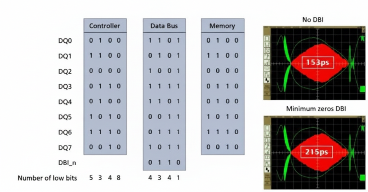
Because POD drivers consume little or no current when the data bus is at a high logic level, reducing the number of low bits on each data transfer lowers power consumption. DBI is a technique that inverts all bits on a bus when doing so increases the number of high bits.
For example, on an 8-bit DQ bus, if at least five bits are low, the controller can invert all eight bits and assert the DBI signal to indicate inversion. The DBI signal is low when inversion has occurred (high indicates no inversion). With a 9-signal grouping (8 DQ signals plus 1 DBI), this technique ensures at least five high states in many transfers, reducing dynamic power consumption.
Reference Voltage (Vref)
DDR signal receivers determine logic levels by comparing input signals against reference voltages (Vref). In DDR4, VREFCA remains similar to DDR3 and is typically generated via external resistor dividers or power-control devices. VREFDQ, however, is generated internally by the DRAM device rather than being provided externally, which reduces board design complexity and frees PCB routing space.
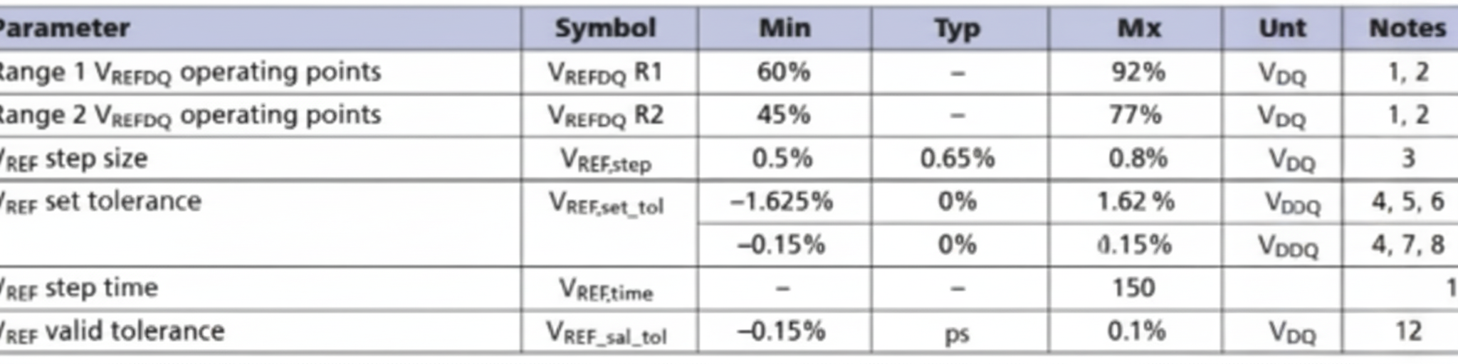
Internal VREFDQ is adjusted via a mode register (MR6). Relevant parameters include voltage range, step size, VREF step time, and VREF full step time. These parameters affect how VREFDQ is calibrated at each power-up.
At each power-up, the memory controller performs calibration sequences to adjust VREFDQ for the DRAM input data lines, optimizing timing and voltage margins. VREFDQ depends not only on VDD but also on trace characteristics and receiver chip properties, so its calibrated value may vary on each power cycle.
Summary
- Higher speed and bandwidth: DDR4 supports higher data transfer rates, typically measured in MT/s (for example, starting around 2133 MT/s and commonly up to 3200 MT/s), which provides faster data access and improved system performance.
- Lower voltage: DDR4 operates at 1.2 V versus DDR3 at 1.5 V, reducing power consumption and heat dissipation—important for mobile and battery-powered systems.
- Higher density: DDR4 supports higher module densities, allowing greater memory capacity per module, which benefits servers and high-performance computing tasks.
- Improved internal efficiency: Bank group design and increased prefetching improve internal throughput and effective memory frequency.
- Error detection and integrity features: DDR4 includes support for ECC, CRC, CA parity, and other mechanisms to improve data reliability and signal integrity.