1. Introduction
When buying DDR memory modules, you may see labels such as DDR3-1066 or DDR3-2400. What do these names mean? The model number indicates the DDR generation and the data rate or clock rate. For example, DDR3-1066 denotes third-generation double data rate synchronous DRAM operating at 1066 MHz. Because DDR transfers data on both the rising and falling edges of the clock, the I/O clock on the module interface is half the effective data rate clock.
2. DDR chip model example
DDR memory modules are assembled from multiple DDR chips. Using the chip model MT41J256M16RH-125 as an example:
Bit width: From 256M16RH we know the chip bus width is 16 bits.
Memory capacity: For MT41J256M16RH-125, capacity is 256M × 16 bits, which equals 512 MB.
I/O clock frequency: From the speed grade suffix "-125" we find tCK = 1.25 ns, so the maximum I/O clock frequency is 1 / 1.25 ns = 800 MHz. This I/O clock is the DDR3 I/O frequency.
Core frequency: The DDR3 I/O interface clock is four times the core frequency, so the DDR3 core frequency is 200 MHz. DDR2 prefetches 4 words into the IO buffer and used a different internal/external clock relationship; DDR3 prefetches 8 words, making the chip clock four times the core frequency.
Data rate: DDR transfers on both clock edges, so each data line transfers at twice the I/O clock frequency: for an 800 MHz I/O clock, that is 1600 MT/s. MT/s stands for Million Transfers Per Second.
Transfer rate per data line: Because data is transferred on both edges, a single data line has an effective transfer rate of 2 × 800 MHz = 1600 Mbit/s.
Theoretical bandwidth: Theoretical bandwidth = transfer rate × bit width × number of chips. For this example: 1600 Mbit/s × 16 bits × 4 chips = 12.8 GB/s.
Effective bandwidth: Effective bandwidth is typically lower due to protocol and timing overhead. If we multiply the theoretical bandwidth by 0.8 as an illustrative efficiency factor, we get 12.8 GB/s × 0.8 = 10.24 GB/s.
This effective bandwidth represents an ideal maximum under simple assumptions; real-world sustained bandwidth depends on access patterns and memory addressing.
3. Xilinx 7-Series FPGA Supported DDR Rates
Supported maximum DDR rates for Xilinx 7-series devices are summarized below for different families.
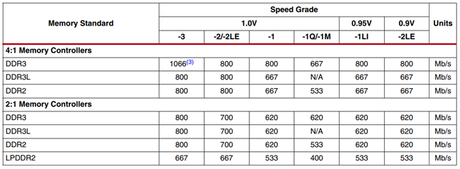
Artix-7 series FPGAs supported maximum DDR rates table.
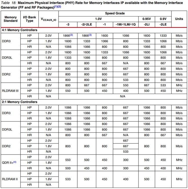
Kintex-7 series FPGAs supported maximum DDR rates table.
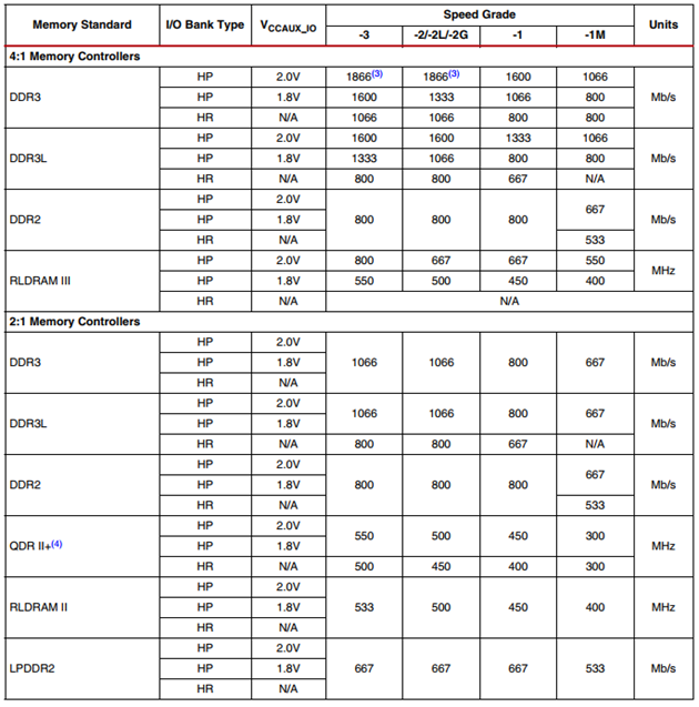
Virtex-7 series FPGAs supported maximum DDR rates table.
4. Conclusion
This article summarized the method for calculating DDR3 bandwidth, including interpretation of chip markings, clock and data rate relationships, and basic bandwidth calculations.