Overview
EEPROM (Electrically Erasable Programmable Read-Only Memory) is a nonvolatile memory that can be electrically erased and reprogrammed. It retains data when power is removed. EEPROM can be erased and reprogrammed on a computer or with dedicated equipment. It is commonly used in plug-and-play applications.
Unlike EPROM, EEPROM can be modified without removing the chip from the system. Because EEPROM may be repeatedly programmed while the system is in use, endurance is an important design consideration.
This article uses the EEPROM on the SANXIN-B04 board as an example. The device used is the 24LC64.
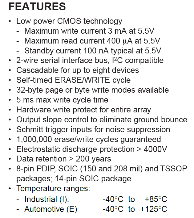
Key specifications
- Two-wire serial bus using the I2C protocol.
- Supports internal erase/write cycles.
- Page write up to 32 bytes and single-byte write modes.
- Maximum write cycle time up to 5 ms.
With these characteristics in mind, we continue with the device datasheet.
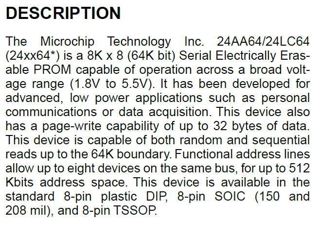
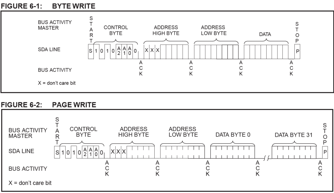
The 24LC64 is organized as 8K x 8, with a total capacity of 64 Kbit. Because the memory depth is 8K locations, addresses range from 0 to 8191, so the address width is 13 bits. This is why the write timing diagram shows a high-byte address and a low-byte address. The device supply range is 1.8 V to 5.5 V. Page write supports up to 32 bytes. Up to eight devices may share the same I2C bus.
Pin functions
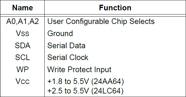
The A0, A1, and A2 pins are device address inputs. When these pins match the slave address bits, the device is selected. These pins must be tied either to VCC or GND as required by the circuit.
SDA is a bidirectional line used for both address and data transfer. Data on SDA is only valid when SCL is high. SDA may change only while SCL is low; a change of SDA while SCL is high is interpreted as a START or STOP condition.
SCL is the serial clock provided by the master to synchronize data transfers.
The WP pin is the write protect input. It may be tied to ground, VCC, or left floating. If left floating, an internal pull-down resistor keeps the device in the non-protected state. When tied to VCC, write operations are disabled while read operations remain allowed.
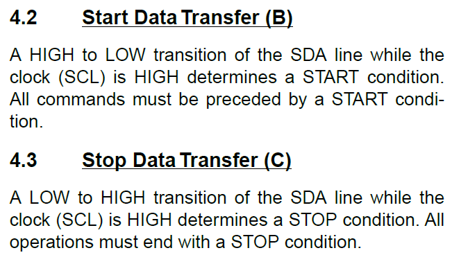
A START condition is defined as SDA going low while SCL is high. All commands follow a START condition.
A STOP condition is defined as SDA going high while SCL is high. All operations end with a STOP condition.
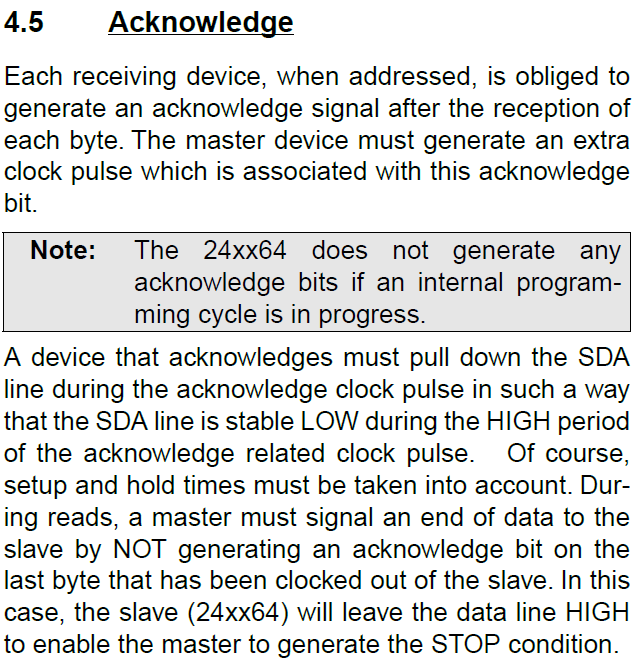
After every 8-bit transfer, the receiver must generate an acknowledge (ACK) by pulling SDA low during the ninth clock pulse. If the device is busy with an internal write cycle, it will not generate an ACK. The ACK must be pulled low while SCL is high and remain stable while SCL is low.
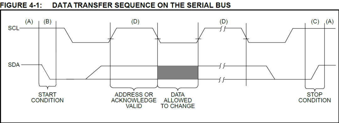
The diagram above shows the I2C bus timing. START and STOP conditions are described above. Address and data bits are sampled while SCL is high. Data bits should only change while SCL is low.
Summary of bus rules
- START condition: SCL high, SDA transitions high to low.
- STOP condition: SCL high, SDA transitions low to high.
- Data is sampled while SCL is high.
- Data changes while SCL is low.
- In the schematic used here, A0, A1, A2, and WP are all tied to ground, so they are ignored in the code.
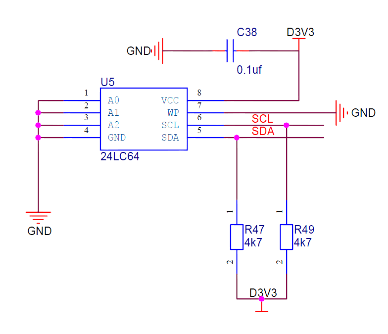
The schematic shows that only SCL and SDA are used to control the EEPROM in this design.
Design framework
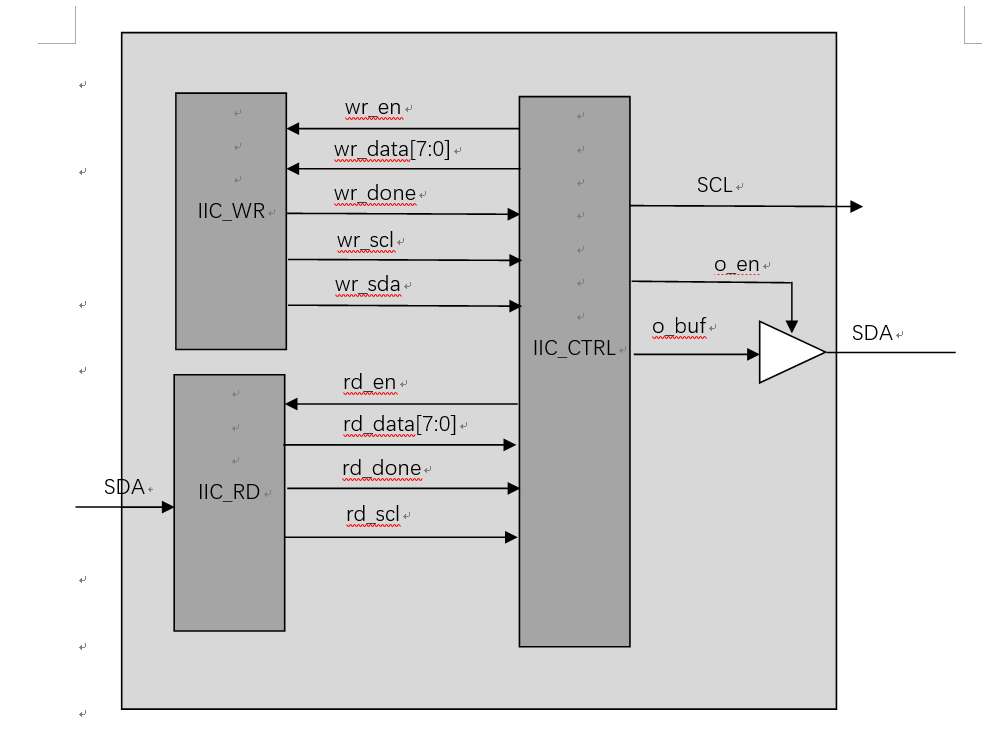
Follow the framework above to implement the modules. The top-level design includes a seven-segment display module to show data read from the EEPROM.
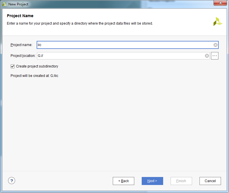
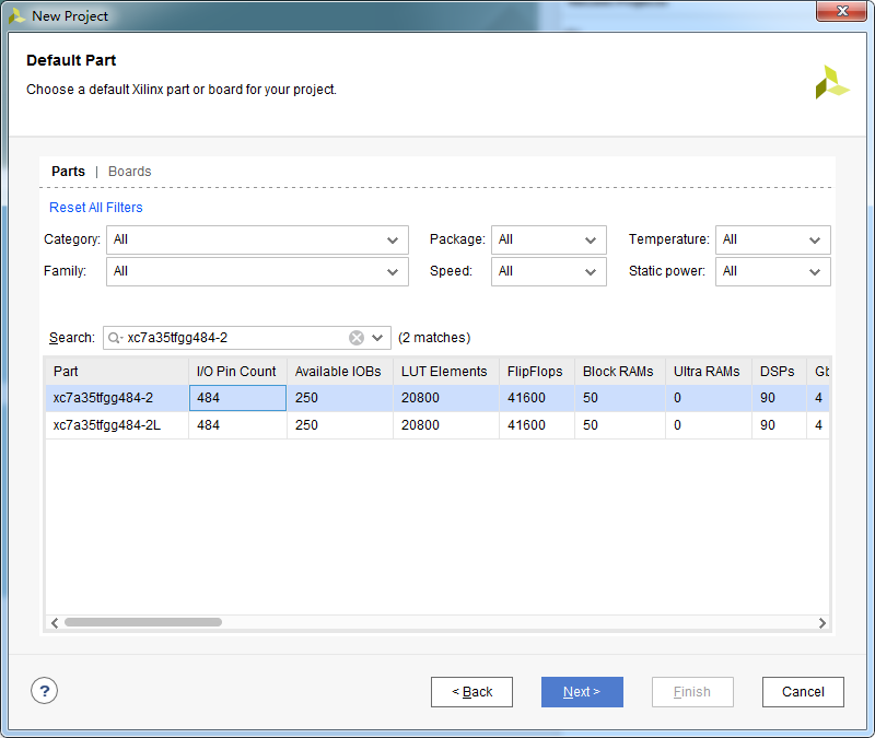
Project setup
After creating the project and source files, start coding the modules.
Write timing
The example below implements single-byte writes. The write state machine sends 8 bits and then reads an ACK. To simplify timing, we treat one quarter of an SCL period as unit time T, so an 8-bit transfer requires counting 32 T units.
Write module (Verilog)
module iic_wr( input wire clk, input wire rst_n, input wire wr_en, input wire [7:0] wr_data, output reg wr_scl, output reg wr_sda, output wire wr_done ); parameter f_clk = 50_000_000; parameter f = 100_000; parameter t = f_clk / f / 4; reg [11:0] cnt; always @ (posedge clk or negedge rst_n) begin if(rst_n == 1'b0) cnt <= 12'd0; else if(wr_en) begin if(cnt == 32 * t - 1) cnt <= 12'd0; else cnt <= cnt + 1'b1; end else cnt <= 12'd0; end always @ (posedge clk or negedge rst_n) begin if(rst_n == 1'b0) begin wr_scl <= 1'b0; wr_sda <= 1'b0; end else if(wr_en) case(cnt) 0 : begin wr_scl <= 1'b0; wr_sda <= wr_data[7]; end 1 * t - 1 : begin wr_scl <= 1'b1; end 3 * t - 1 : begin wr_scl <= 1'b0; end 4 * t - 1 : begin wr_sda <= wr_data[6]; end 5 * t - 1 : begin wr_scl <= 1'b1; end 7 * t - 1 : begin wr_scl <= 1'b0; end 8 * t - 1 : begin wr_sda <= wr_data[5]; end 9 * t - 1 : begin wr_scl <= 1'b1; end 11* t - 1 : begin wr_scl <= 1'b0; end 12* t - 1 : begin wr_sda <= wr_data[4]; end 13* t - 1 : begin wr_scl <= 1'b1; end 15* t - 1 : begin wr_scl <= 1'b0; end 16* t - 1 : begin wr_sda <= wr_data[3]; end 17* t - 1 : begin wr_scl <= 1'b1; end 19* t - 1 : begin wr_scl <= 1'b0; end 20* t - 1 : begin wr_sda <= wr_data[2]; end 21* t - 1 : begin wr_scl <= 1'b1; end 23* t - 1 : begin wr_scl <= 1'b0; end 24* t - 1 : begin wr_sda <= wr_data[1]; end 25* t - 1 : begin wr_scl <= 1'b1; end 27* t - 1 : begin wr_scl <= 1'b0; end 28* t - 1 : begin wr_sda <= wr_data[0]; end 29* t - 1 : begin wr_scl <= 1'b1; end 31* t - 1 : begin wr_scl <= 1'b0; end default : ; endcase end assign wr_done = (cnt == 32 * t - 1) ? 1'b1 : 1'b0; endmodule
Read module (Verilog)
module iic_rd( input wire clk, input wire rst_n, input wire rd_sda, input wire rd_en, output reg rd_scl, output reg [7:0] rd_data, output wire rd_done ); parameter f_clk = 50_000_000; parameter f = 100_000; parameter t = f_clk / f / 4; reg [11:0] cnt; always @ (posedge clk or negedge rst_n) begin if(rst_n == 1'b0) cnt <= 12'd0; else if(rd_en) begin if(cnt == 32 * t - 1) cnt <= 12'd0; else cnt <= cnt + 1'b1; end else cnt <= 12'd0; end always @ (posedge clk or negedge rst_n) begin if(rst_n == 1'b0) begin rd_scl <= 1'b0; rd_data <= 8'd0; end else if(rd_en) case(cnt) 0 : begin rd_scl <= 1'b0; end 1 * t - 1 : begin rd_scl <= 1'b1; end 2 * t - 1 : begin rd_data[7] <= rd_sda; end 3 * t - 1 : begin rd_scl <= 1'b0; end 5 * t - 1 : begin rd_scl <= 1'b1; end 6 * t - 1 : begin rd_data[6] <= rd_sda; end 7 * t - 1 : begin rd_scl <= 1'b0; end 9 * t - 1 : begin rd_scl <= 1'b1; end 10* t - 1 : begin rd_data[5] <= rd_sda; end 11* t - 1 : begin rd_scl <= 1'b0; end 13* t - 1 : begin rd_scl <= 1'b1; end 14* t - 1 : begin rd_data[4] <= rd_sda; end 15* t - 1 : begin rd_scl <= 1'b0; end 17* t - 1 : begin rd_scl <= 1'b1; end 18* t - 1 : begin rd_data[3] <= rd_sda; end 19* t - 1 : begin rd_scl <= 1'b0; end 21* t - 1 : begin rd_scl <= 1'b1; end 22* t - 1 : begin rd_data[2] <= rd_sda; end 23* t - 1 : begin rd_scl <= 1'b0; end 25* t - 1 : begin rd_scl <= 1'b1; end 26* t - 1 : begin rd_data[1] <= rd_sda; end 27* t - 1 : begin rd_scl <= 1'b0; end 29* t - 1 : begin rd_scl <= 1'b1; end 30* t - 1 : begin rd_data[0] <= rd_sda; end 31* t - 1 : begin rd_scl <= 1'b0; end default : ; endcase end assign rd_done = (cnt == 32 * t - 1) ? 1'b1 : 1'b0; endmodule
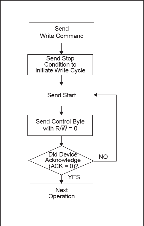
Control module and ACK handling
The control module implements a state machine to execute data writes and to evaluate ACK responses. The START condition and STOP condition are implemented by manipulating SDA and SCL according to the timing rules described earlier.
To read ACK, sample SDA at the center of SCL high. If the sampled ACK is 0, the device responded correctly and the state machine proceeds. If it is not 0, return to the START state and retry.
Top-level considerations
At the top level, use tri-state control for the bidirectional SDA line so multiple drivers do not drive the bus simultaneously.

Simulation
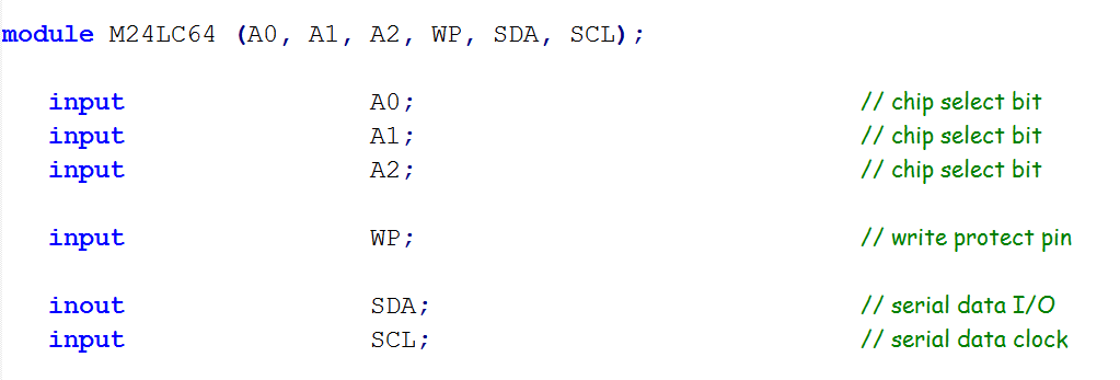
When simulating, simply observing signals may not show a correct ACK because the modeled device will not ACK while it simulates an internal write cycle. Therefore, instantiate an EEPROM model in the simulation testbench and connect the model's control pins to the simulated bus.
Note that the write cycle in the model is defined as 5 ms. If this is too long for your simulation, adjust the model parameters as needed.

Testbench example (Verilog)
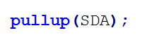
`timescale 1ns/1ps module iic_tb; reg clk; reg rst_n; reg key; wire [2:0] sel; wire [7:0] seg; wire SCL; wire SDA; defparam iic_inst.jitter_inst.t = 10; pullup(SDA); initial begin clk = 0; rst_n = 0; key = 1; #100; rst_n = 1; #1000; key = 0; #1000; key = 1; #1000000; $stop; end always #10 clk = ~clk; iic iic_inst( .clk (clk), .rst_n (rst_n), .key (key), .sel (sel), .seg (seg), .SCL (SCL), .SDA (SDA) ); M24LC64 M24LC64_inst( .A0 (1'b0), .A1 (1'b0), .A2 (1'b0), .WP (1'b0), .SDA (SDA), .SCL (SCL) ); endmodule
Simulation notes and results
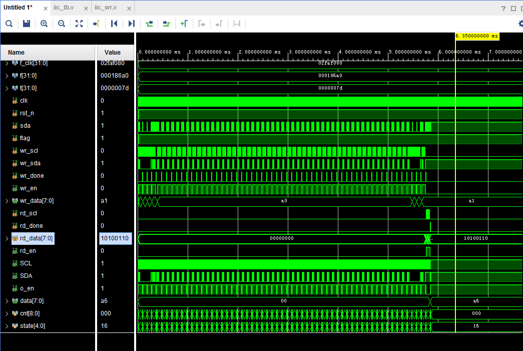
In the simulation waveform, the data read back matches the data written, indicating the driver functions correctly. During the device write cycle, the device will not accept new commands and will not ACK until the write completes. This causes the bus to repeatedly see START, control byte, and missing ACK cycles until the model finishes the internal write, at which point an ACK is returned and the state machine proceeds to completion.
Because the simulated SDA line floats when released, pull-ups are required in the simulation to display correct high levels. Add pull-ups as needed to observe correct bus behavior.
With the above setup and the device model in place, the driver and simulation behave as expected.