Overview
Memory endurance is defined as the number of times a storage cell can be written or erased. For applications that require strict and long-term data integrity, memory endurance is a critical system performance characteristic and a key design consideration. Ferroelectric RAM, or FRAM, is a fast, nonvolatile, low-power memory technology whose high endurance is one of its principal advantages compared with other nonvolatile memories based on floating-gate or phase-change technologies. FRAM "endurance" refers to the ability to retain the nonvolatile component of the ferroelectric switching charge after fatigue, i.e., the memory state retention after many switching cycles.
Mechanisms of Fatigue
Extensive research has investigated the origins of switching charge (polarization) loss in materials after large numbers of switching cycles. Several mechanisms have been proposed, including oxygen vacancies, suppression of opposite domains near the ferroelectric-electrode interface, and spatial distribution of internal bias fields. These mechanisms can lead to domain pinning in the ferroelectric, which reduces the switching charge density as switching cycles accumulate.
Process Nodes and Measured Endurance
FRAM manufacturing has progressed across multiple process nodes, such as 0.5 μm, 0.35 μm, and 0.13 μm. Endurance characteristics vary by generation. Although FRAM exhibits strong endurance at each node, devices built on the 0.13 μm node have demonstrated exceptional endurance, reaching up to 10^13 cycles historically and now up to 10^15 cycles. At the 0.13 μm node, measuring the practical maximum endurance within a reasonable time presents challenges: it requires extensive test time and innovative test methods to determine the true endurance limit of 0.13 μm FRAM products.
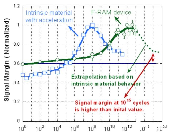
Figure 1. The signal margin versus cycles for FRAM devices and the intrinsic material shows that the signal margin at 10^15 cycles remains higher than the initial value.
Device-Level and Material-Level Observations
Current specifications for 10^15-cycle endurance on 0.13 μm FRAM are based on preliminary evaluation of a sample of 1,280-bit FRAM arrays built with the 0.13 μm node. Figure 1 shows that device-level signal margin reaches a maximum between 10^12 and 10^13 cycles. Extrapolating device-level endurance beyond 10^13 cycles is possible using similar curves observed at the intrinsic material level. The extrapolated device-level endurance, indicated by the dashed line in Figure 2, suggests that the remaining signal margin after 10^15 cycles is still higher than the initial margin (the minimum-cycle signal margin). This indicates sufficient signal margin to ensure device reliability after 10^15 cycles, consistent with the endurance specifications for 0.13 μm FRAM foundries.