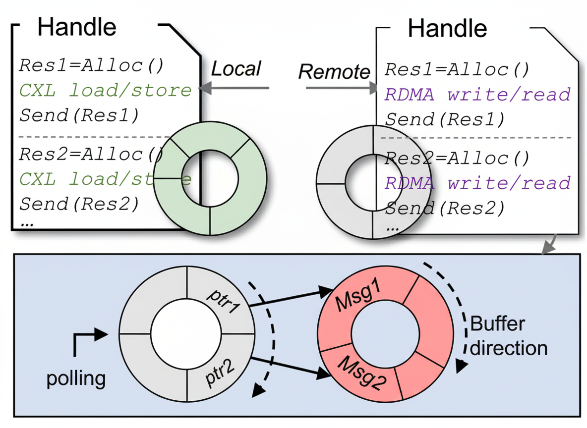
Key points
- DRAM operation explained with diagrams, including read, write, and storage.
- Why DRAM is relatively cheap while SRAM is more expensive.
Introduction
Memory is a fundamental topic for hardware engineers. Even moderately complex systems require DRAM, which is one of the most complex and costly components after the CPU. Design, simulation, debugging, and board-level work for DRAM are all complex and important. Familiarity with DRAM use directly affects the quality of system design. This article uses accessible diagrams and text to explain the basic operating principle of a single DRAM circuit cell.
What is DRAM
DRAM (dynamic random access memory) is the dynamic form of random access memory commonly used for computer and mobile device main memory. The article describes in detail how DRAM stores and reads data.
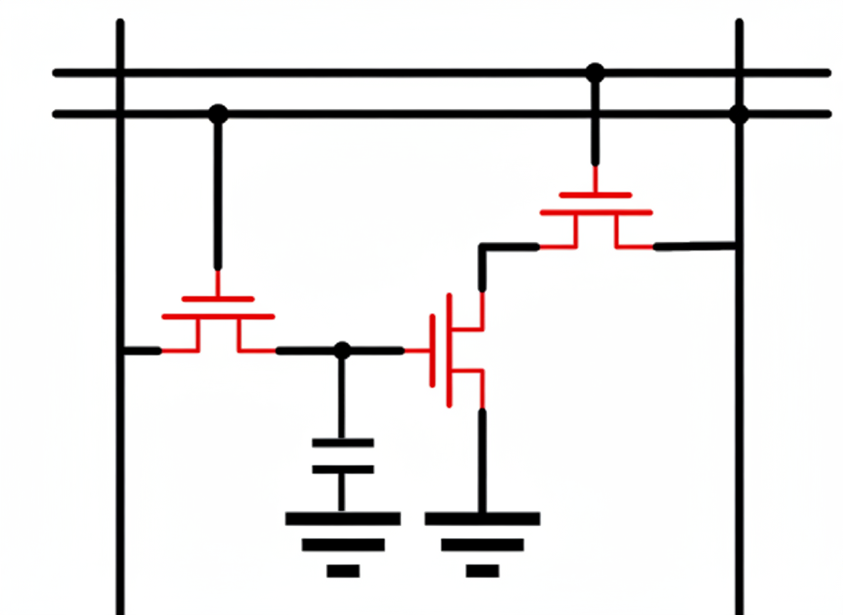
1. The single-transistor DRAM cell
The single-transistor DRAM cell is the standard choice for high-density memory. The circuit consists of an access transistor and a storage capacitor, as shown below. The capacitor stores charge representing a logic 1 when charged and logic 0 when discharged.
Two basic premises to keep in mind: first, the voltage on the storage capacitor is referenced around Vcc/2; second, electrons carry negative charge, so a greater number of electrons corresponds to lower electric potential. To help visualization, the article uses a water-reservoir analogy where the reservoir top is defined as 0 V and the bottom as Vcc.
Three basic operations of a DRAM cell
The three basic operations are storing, writing, and reading data. For clarity, each process is compared to filling or draining a water reservoir.
Storing data
When the reservoir gate is closed (row address/wordline at 0 V), water cannot flow out of the reservoir and upstream water cannot flow in, so the reservoir level remains unchanged and information is retained. The water level corresponds to a logic level.
Writing data
Writing can be split into writing a 0 and writing a 1. The following describes writing a 0.
Sequence:
- Before writing, the cell may contain either charge or no charge.
- The column line is driven to the desired level (the source of data). For writing 0 in the analogy, the upstream channel is set to a high water level corresponding to a low electrical potential on the column line (for example, column line at 0 V).
- The row wordline is asserted (row line driven high) to open the gate. The small amount of water in the reservoir then equalizes with the upstream channel, filling or emptying the reservoir according to the column-level, so the cell becomes the intended logic state.
The canal lock analogy for passing cargo through a lock is also applicable and may help with intuition.
Reading data
DRAM reads typically use column precharge to Vcc/2. The following describes reading a 0.
Procedure:
- The cell is charged to its stored state (for example, full reservoir for logic 0, 0 V potential in the analogy).
- The bitline is precharged to Vcc/2.
- The row wordline is asserted, connecting the small cell capacitor to the large bitline capacitance. Because the cell capacitor is much smaller than the bitline capacitance, the cell only causes a small voltage perturbation on the bitline.
- The sense amplifier detects this small delta and amplifies it to a full logic level, identifying whether the cell held a 0 or 1.
The voltage change can be approximated as delta = (Vbitline_initial - Vcell) * Cb / (Cb + Cs) where Cb is the bitline capacitance and Cs is the cell capacitance. The bitline capacitance is much larger than the cell capacitance, so the resulting voltage change is small and requires amplification. The real process involves many additional timing and circuit details, but this analogy conveys the essential principle.
Because the cell capacitor loses charge over time due to leakage, periodic refresh operations are required to restore the charge. This is the origin of the term dynamic in DRAM.
2. Why SRAM is more expensive than DRAM and their differences
SRAM is well known to be more expensive than DRAM. Because of that cost difference, DRAM is used for higher-capacity main memory while SRAM is used for smaller, faster caches. The main reasons for the price and performance differences are:
- SRAM is faster but uses much more silicon area per bit. SRAM cells typically use six transistors per bit, so SRAM has lower density and higher cost per bit compared with single-transistor DRAM cells.
- SRAM consumes static power and generates more heat because of the larger transistor count, which limits large-area use. DRAM, by contrast, requires refresh circuitry to maintain data, and the refresh activity also consumes significant power, especially in standby scenarios.
Historically, there have been alternative DRAM cell topologies. The article shows an example of an early alternative structure; comparing the tradeoffs of different cell designs can be instructive.
Summary: Practical notes for DRAM cell usage
- Understand the basic DRAM cell: one storage capacitor and one access transistor. Correct read and write timing is essential.
- Data reliability during read requires sensitive sense amplifiers because the voltage change from the cell is very small. Factors such as temperature and noise affect sensing, so techniques like differential amplification and reference voltages are used to improve reliability.
- Avoid applying excessive voltages to DRAM cells to prevent capacitor damage. Excessive or unnecessary read/writes accelerate wear.
- DRAM requires periodic refresh operations to maintain stored data. Ensure the refresh mechanism is correctly implemented and scheduled.
- Layout and signal integrity matter: place DRAM circuits to minimize interference and noise, and select timing and clock frequencies that meet DRAM timing specifications for stability and reliability.