Overview
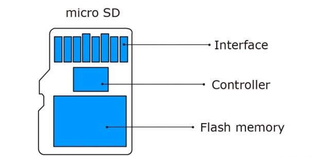
Many modern NAND flash devices use an integrated architecture that places the interface, controller, and memory die inside a single ceramic layer. This is known as an integrated package.
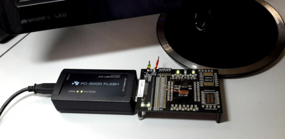
Until recently, most memory cards such as SD, Sony MemoryStick, and MMC used a classic design composed of separate parts: a controller, a printed circuit board, and a NAND memory chip in a TSOP48 or LGA-52 package. In those cases, recovery was straightforward: the memory chip was desoldered and read directly with a tool such as PC-3000 FLASH, following the same preparation used for USB flash drives.
When a storage card or USB flash device is based on an integrated package architecture, the approach is different. How can you access the NAND memory die and read data in that case?
Expose the Technical Pins
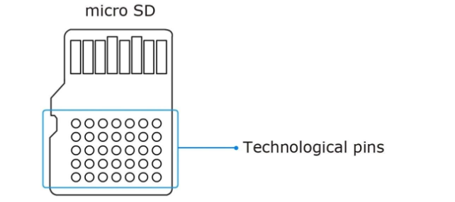
In integrated-package devices, the usual method is to remove the ceramic coating from the bottom to reveal special technology pads or pins. This process is delicate and requires careful sanding to avoid damaging the pin layer; any damage can make data recovery impossible.
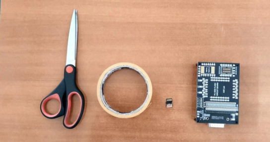
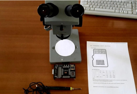
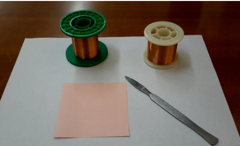
Required Tools and Materials
Before starting, note that working with integrated flash devices requires strong soldering skills and specialized equipment. If you have not previously attempted soldering integrated flash devices, practice on expendable units first. The required equipment includes:
- Optical microscope with x2, x4, x8 zoom
- USB soldering iron with a very thin, sharp tip
- Double-sided tape
- Liquid flux
- BGA flux
- Hot air gun (for example, Lukey 702)
- Rosin
- Wooden toothpicks
- Isopropyl alcohol (75% purity or higher)
- 0.1 mm diameter copper wire, enamelled wire
- Jewelry-grade sandpaper (1000, 2000, 2500 grit)
- BGA solder balls, 0.3 mm
- Tweezers
- Sharp scalpel
- Schematics and pinout diagrams
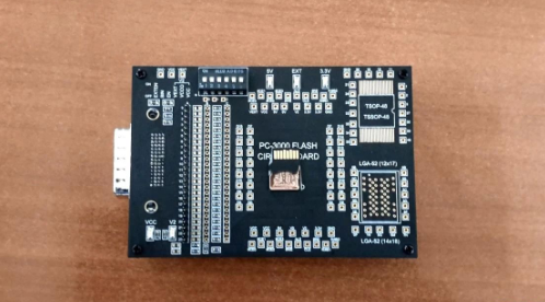
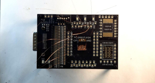
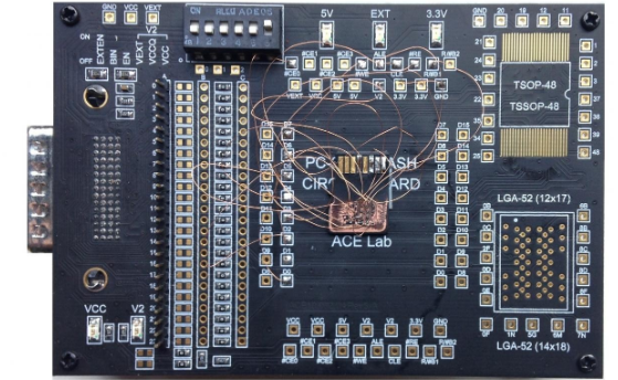
- PC-3000 Flash board adapter
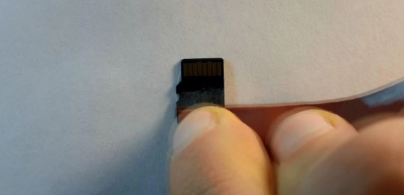
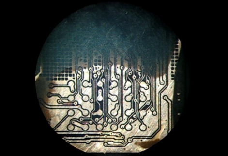
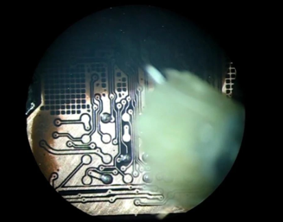
Preparation and Sanding
Fix the integrated flash device to the work surface with double-sided tape. Begin removing the ceramic coating from the bottom. This operation takes time and requires patience. Start with coarse sandpaper (1000 or 1200 grit).
When the bulk of the coating is removed, switch to finer sandpaper, around 2000 grit.
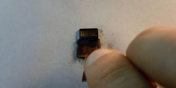
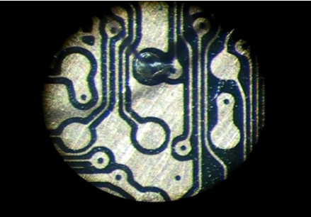
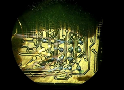
Finally, use the finest grit, about 2500, until the copper contact layer is visible.
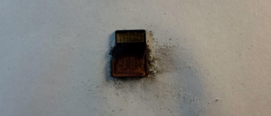
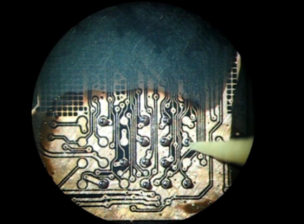
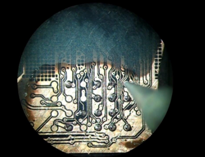
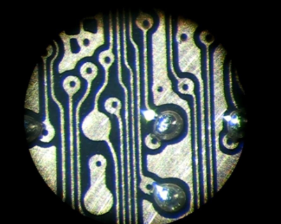
If performed correctly, the exposed contacts should look like this:
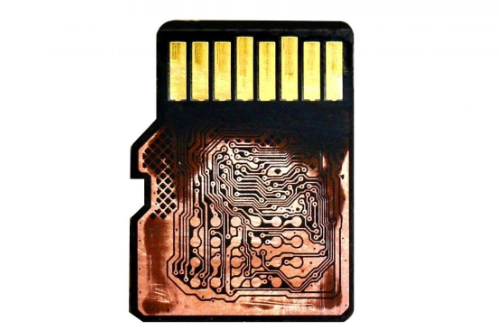
Identify and Prepare Pinouts
Locate the pinout for the specific integrated flash device. To access the die directly while keeping the package intact, three groups of contacts typically need to be wired:
- Data I/O: D0, D1, D2, D3, D4, D5, D6, D7
- Command/control signals: ALE, RE, R/B, CE, CLE, WE
- Power: VCC, GND
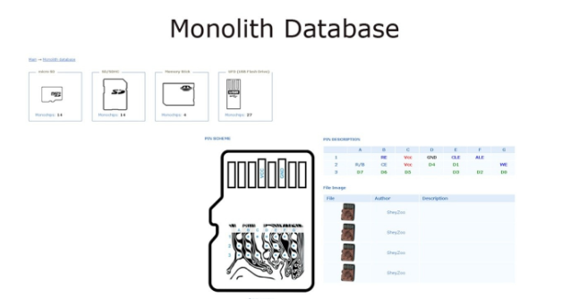
Select the correct device category (for example, microSD) and the compatible pinout type. Mount the device on the PCB adapter to make soldering easier.
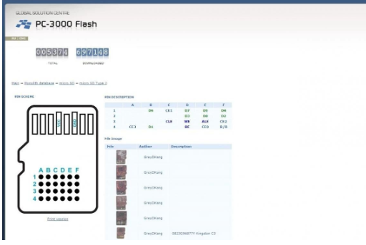
Print the pinout diagram and keep it at hand during soldering for reference.
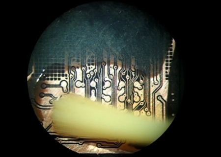
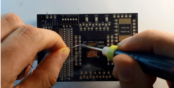
Soldering BGA Balls to Contacts
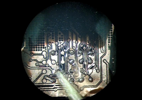
Under a microscope, apply a drop of liquid flux to the exposed contacts. Using a small pick, place BGA solder balls on the copper pads according to the pinout. Use solder balls sized at about 75% of the pad diameter. Liquid flux will help hold the balls in place.
Gently touch each solder ball with the soldering iron tip to melt them. Take care to perform this step gently and precisely.
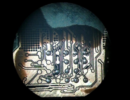
After melting, apply BGA flux over the contacts. Use a hot air gun to heat the pins to about 200°C. BGA flux helps distribute heat and ensures the solder forms proper hemispherical contacts.
Clean all flux residues with isopropyl alcohol and a brush.
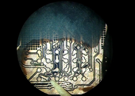
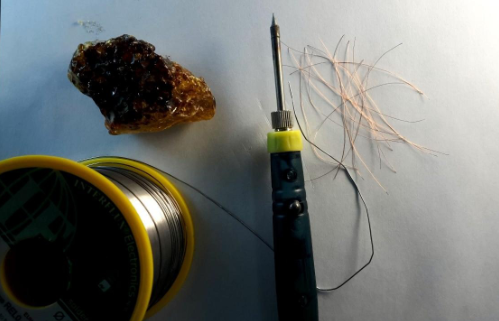
Prepare and Solder Wires
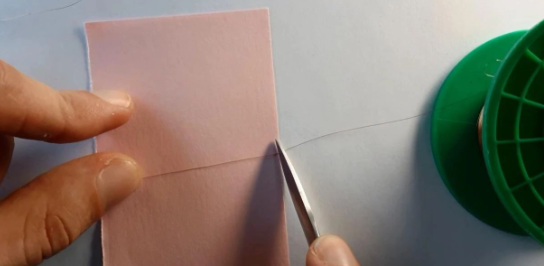
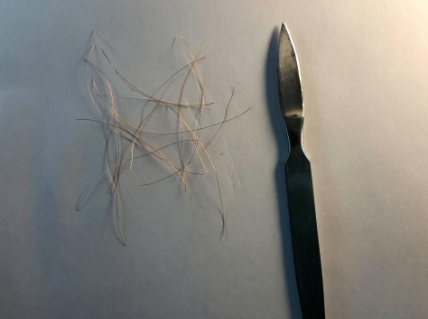
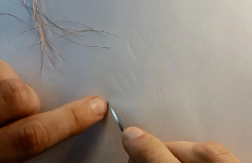
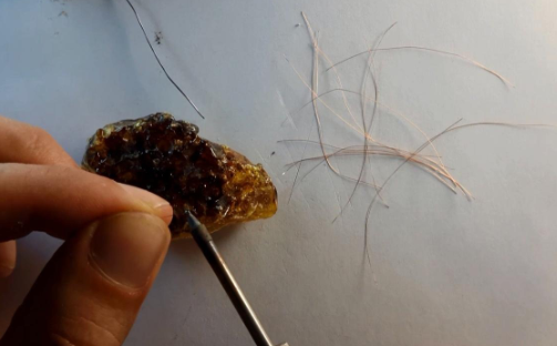
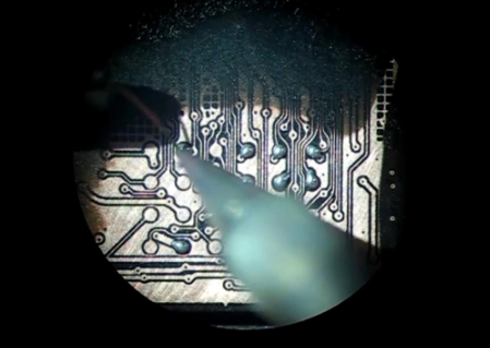
Prepare copper wires of equal length, about 5–7 cm. Use a paper strip as a length guide to cut matching pieces. Score the enamel insulation slightly on both ends with a scalpel to remove it, then tin the exposed copper with rosin solder.
Start soldering the wires to the board adapter side first, then under the microscope solder the other ends to the BGA contacts on the integrated device. This is the most delicate step and requires precise, steady work. Keep the soldering iron tip clean and re-tin as needed.
After soldering all wires, verify that no contact is shorted to the ground plane. All pins should be secure and isolated.
Final Steps
Connect the PCB adapter to the reading tool such as PC-3000 FLASH and begin the reading process.