The primary role of the memory subsystem is to deliver the required data or instructions to the host (CPU or GPU) as quickly and reliably as possible across a wide range of applications such as cloud computing, artificial intelligence (AI), automotive, and mobile. SoC designers can choose from several memory technologies, each with different characteristics and advanced features. Double data rate (DDR) synchronous dynamic random-access memory (DRAM) has become the dominant main system memory technology because it uses capacitors as storage elements to provide high density, relatively simple architecture, low latency, high performance, unlimited write endurance for the cells, and low power consumption.
Choosing the right memory technology is often the most critical decision for achieving optimal system performance. This article introduces different memory technologies to help SoC designers select the memory solution that best meets their application requirements.
DDR DRAM Standards
Designers keep adding more cores and functions to their SoCs, yet improving performance while maintaining low power and small silicon area remains essential. DDR SDRAM (referred to as DRAM) meets these needs by offering dense, high-performance, and low-power memory solutions in DIMMs or discrete DRAM devices. JEDEC defines and develops three DRAM standard categories to help designers meet power, performance, and specification targets:
Standard DDR
Targeted at servers, cloud computing, networking, laptops, desktops, and consumer applications, standard DDR supports wider channel widths, higher densities, and various form factors. Since 2013, DDR4 has been the most widely used standard in this category; DDR5 devices are expected to appear in the near future.
Mobile DDR
Targeted at power- and specification-sensitive areas such as mobile and automotive applications, mobile DDR provides narrower channel widths and several low-power operating states. The most common standard today is LPDDR4, with LPDDR5 devices expected to arrive later.
Graphics DDR
Intended for data-intensive applications that require extremely high throughput, such as graphics, data center acceleration, and AI, graphics DDR includes standards such as GDDR and high bandwidth memory (HBM).
The three DRAM categories above use the same DRAM array and capacitors as the basic storage element. However, each category offers unique architectural features tailored to its target applications, including custom data rates and bus widths, host-to-DRAM connection options, electrical specifications, I/O termination schemes, DRAM power states, and reliability features. Figure 1 shows JEDEC's three DRAM categories.
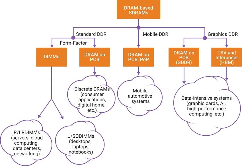
Figure 1: JEDEC defines three DRAM categories to meet various application design requirements
Standard DDR Details
Standard DDR DRAM is common in enterprise servers, data centers, laptops, desktops, and consumer devices, providing high density and performance. DDR4 is the most common standard in this category and offers several advantages over its predecessors DDR3 and DDR3L (the low-power version of DDR3):
- Higher data rates, up to 3200 Mbps compared to DDR3 which ran up to 2133 Mbps.
- Lower operating voltage (1.2 V for DDR4 versus 1.5 V for DDR3 and 1.35 V for DDR3L).
- Improved performance (for example, more banks), lower power (for example, data bus reversal), and enhanced reliability, availability, and serviceability (RAS) features such as post-package repair and CRC.
- Higher density as DRAM die sizes increase from 4 Gb to 8 Gb and 16 Gb.
DDR5 under development by JEDEC is expected to raise data rates to 4800 Mbps while operating at about 1.1 V. DDR5 introduces architectural and RAS features to handle these higher speeds while minimizing system downtime due to memory errors. Key features include on-module voltage regulators, improved refresh schemes, architectures aimed at higher channel utilization, on-DRAM internal error correction code (ECC), more banks to improve performance, and higher capacities.
Mobile DDR
Mobile DDR, also called low-power DDR (LPDDR) DRAM, includes additional features to reduce power consumption, which is critical for battery-powered mobile and automotive applications and for SSD cards. LPDDR can run at higher speeds than standard DDR to deliver performance while providing low-power states to improve energy efficiency and extend battery life.
LPDDR channels are typically 16- or 32-bit wide compared with standard DDR 64-bit channels. Each successive LPDDR generation targets higher performance and lower power than its predecessor, and different LPDDR generations are not mutually compatible.
LPDDR4 is the most common standard in this category and supports data rates up to 4267 Mbps at 1.1 V. LPDDR4 devices are often dual-channel, supporting two x16 (16-bit) channels. Each channel is independent with its own command/address pins, giving system architects flexibility when connecting the SoC host to LPDDR4 DRAM.
LPDDR4X is a variant of LPDDR4 that further reduces power by lowering the I/O voltage (VDDQ) from 1.1 V to around 0.6 V while still supporting up to 4267 Mbps.
LPDDR5 follows LPDDR4/4X and is expected to reach up to 6400 Mbps; it is actively developed in JEDEC. LPDDR5 aims to provide new low-power and reliability features for mobile and automotive applications, including a deep-sleep mode intended to significantly reduce idle power to extend battery life. New architectural features will allow LPDDR5 to run at high speeds with lower operating voltages than LPDDR4/4X.
Graphics DDR
Two different memory architectures for high-throughput applications such as GPUs and accelerators are GDDR and HBM.
GDDR Standards
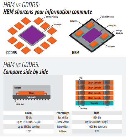
GDDR DRAM is designed for graphics processors and accelerators. Data-intensive systems such as graphics cards, game consoles, and high-performance computing—including automotive, AI, and deep learning—commonly use GDDR. GDDR standards (GDDR6/5/5X) are point-to-point standards that can support rates up to 16 Gbps per pin. GDDR5 served as a discrete DRAM solution supporting up to 8 Gbps; it could be configured to run in a ×32 or ×16 (folded) mode detected during device initialization.
GDDR5X targets 10 to 14 Gbps per pin, nearly double GDDR5. A main difference is that GDDR5X uses a 16N prefetch rather than 8N. GDDR5X uses more package pins per chip (190 pins versus 170 pins for GDDR5), so GDDR5 and GDDR5X require different PCB designs. GDDR6 is the latest GDDR standard, running up to 16 Gbps at a lower voltage of 1.35 V, whereas GDDR5 required 1.5 V for comparable rates.
HBM and HBM2 Standards
HBM offers an alternative to GDDR for GPUs and accelerators. Where GDDR achieves throughput with narrower channels and very high per-pin rates, HBM uses multiple independent channels—typically eight—each with a much wider data path (128 bits per channel) and lower per-pin rates around 2 Gbps. As a result, HBM can deliver high throughput at lower power and with a smaller footprint than GDDR. HBM2 is the most common standard in this category today and supports up to about 2.4 Gbps.
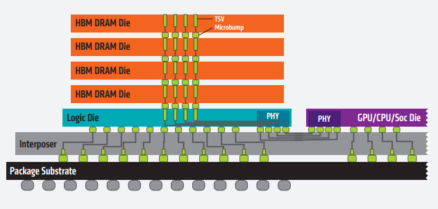
HBM2 DRAM stacks up to eight DRAM dies (including an optional base die) for a smaller overall silicon footprint. Dies are connected via through-silicon vias (TSVs) and microbumps. Common densities include 4 GB or 8 GB per HBM2 package.
Beyond more channels, HBM2 introduces architectural changes to improve performance and reduce bus congestion. For example, HBM2 supports a pseudo-channel mode where each 128-bit channel is split into two 64-bit semi-independent subchannels. They share the channel's row and column command bus but execute commands independently. Increasing the number of channels allows activating more banks per unit time without violating restrictive timing parameters such as tFAW, thereby increasing effective bandwidth. Other features in the standard include optional ECC support that enables 16 error detection bits per 128 bits of data.
HBM3 is expected to appear in the coming years and to offer higher density, greater bandwidth (for example, 512 GB/s), lower voltage, and lower cost. Table 1 shows a high-level comparison between GDDR6 and HBM2 DRAM.
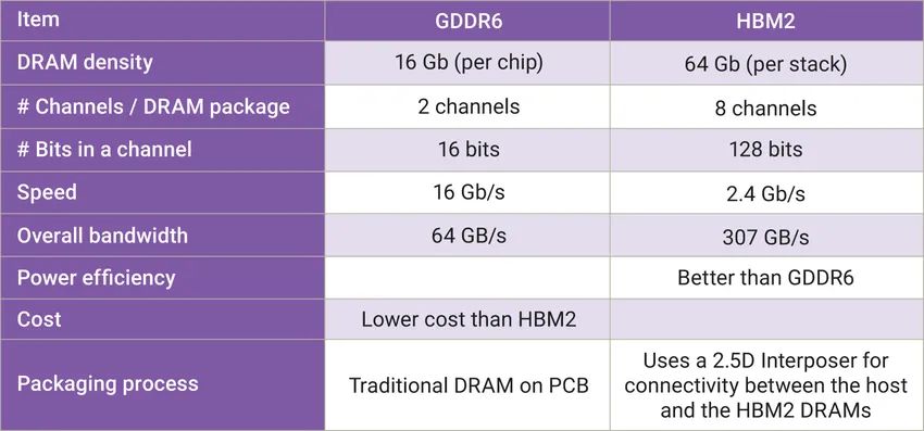
Table 1: High-level comparison of GDDR6 and HBM2 advantages for system architects
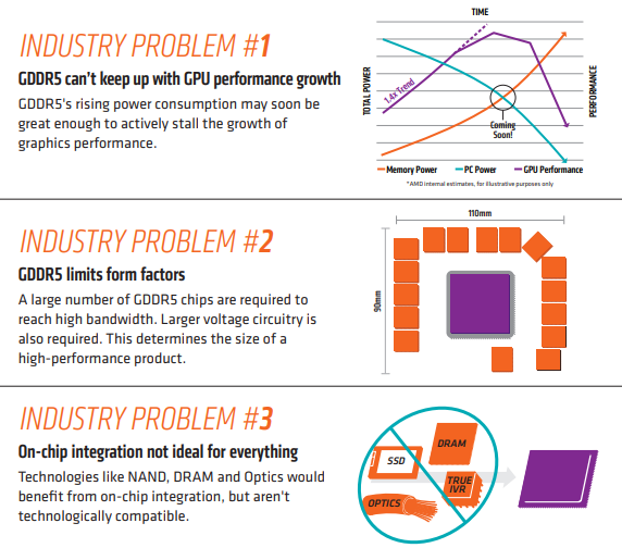
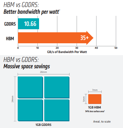
Some industry analysis has noted that GDDR5 may struggle to keep pace with GPU performance growth and that rising GDDR5 power consumption could limit graphics performance scaling. GDDR5 requires more chips and higher circuit voltages to achieve high bandwidth. HBM provides a low-power, ultra-wide communication channel using vertically stacked DRAM dies interconnected by TSVs, enabling performance beyond traditional limits.
HBM reduces communication cost compared with GDDR5, lowers energy per bandwidth, and reduces silicon area, which helps shrink the overall footprint.
Summary
To provide different features and advantages, JEDEC defines three main DDR categories: standard DDR, mobile DDR, and graphics DDR. Standard DDR targets servers, data centers, networking, laptops, desktops, and consumer applications with wider channel widths, higher densities, and multiple form factors. Mobile DDR (LPDDR) targets mobile and automotive applications with strict power and specification requirements, offering narrower channel widths and several low-power states. Graphics DDR addresses applications that require extremely high throughput; JEDEC defines both GDDR and HBM as graphics DDR standards. SoC designers can choose among these memory solutions and standards to meet their target application needs. The selected memory solution affects SoC performance, power consumption, and specification requirements.