Recently, flagship phones from major China manufacturers were released, drawing significant attention in the industry and market. A professional teardown by a research agency found that the main controller and most chips are domestic, while only the LPDDR5 DRAM and NAND flash memory come from SK Hynix. The markings appear as H58GG6MK6GX037 and HN8T25DEHKX077 (the first letter should be H according to SK Hynix naming rules but is obscured by a shield). On SK Hynix's website, the two part numbers are listed as shown below.
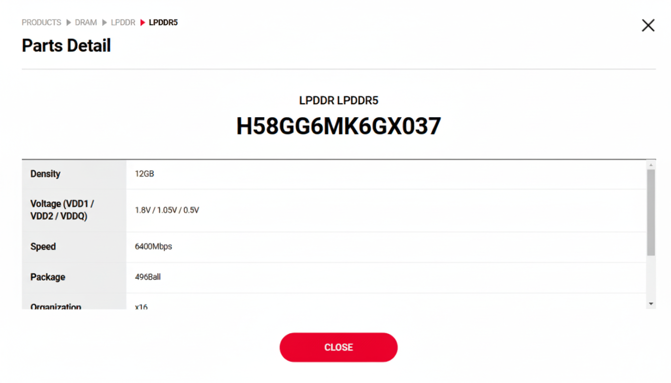
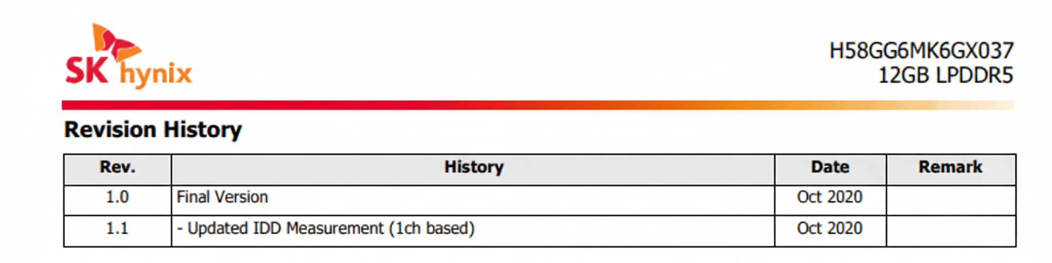
LPDDR5 DRAM: H58GG6MK6GX037
The H58GG6MK6GX037 is a 12GB LPDDR5 DRAM, but its product status on SK Hynix's site is listed as CS rather than MP.
In February 2019, JEDEC officially released the LPDDR5 low-power memory standard, Low Power Double Data Rate 5. Compared with LPDDR4, LPDDR5 I/O speed increases from 3200MT/s to 6400MT/s, doubling the data rate. With a 64-bit bus common in high-end smartphones, this yields 51.2GB/s; with a 128-bit bus as used in some PCs, throughput can exceed 100GB/s.
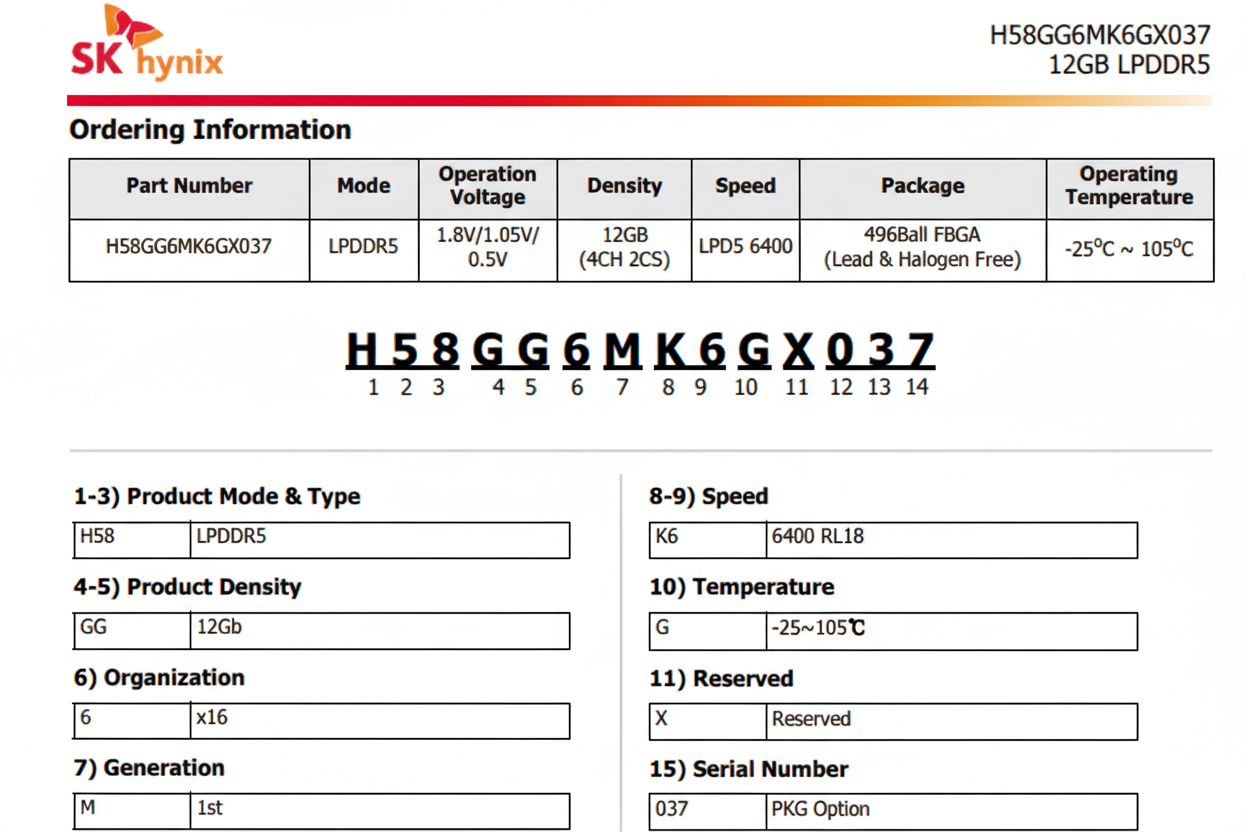
According to SK Hynix's datasheet, the H58GG6MK6GX037 likely entered production around 2021.
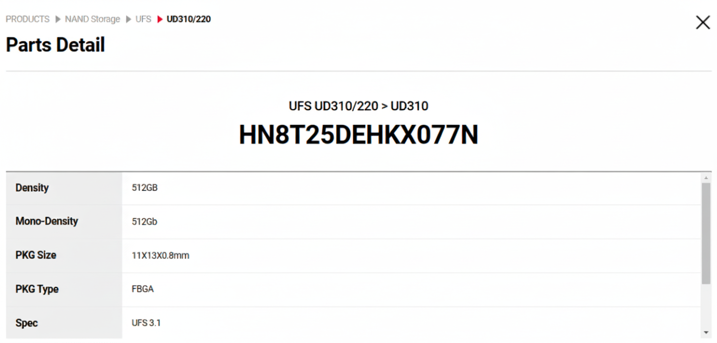
UFS Storage: HN8T25DEHKX077
HN8T25DEHKX077 is a 512GB UFS 3.1 device, and its status is also listed as CS.
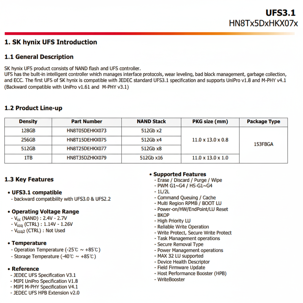
On January 30, 2020, JEDEC published the UFS 3.1 standard. Compared with earlier versions, UFS 3.1 introduced three main updates: "Write Booster" — an SLC non-volatile cache that can improve write performance; "DeepSleep" — a new low-power state that reduces UFS activity and minimizes regulator wake-ups to lower overall power consumption and extend battery life; and "Performance Throttling Notifications" — allowing a UFS device to notify the host when high temperature causes storage performance degradation, with optional host-side throttling support.
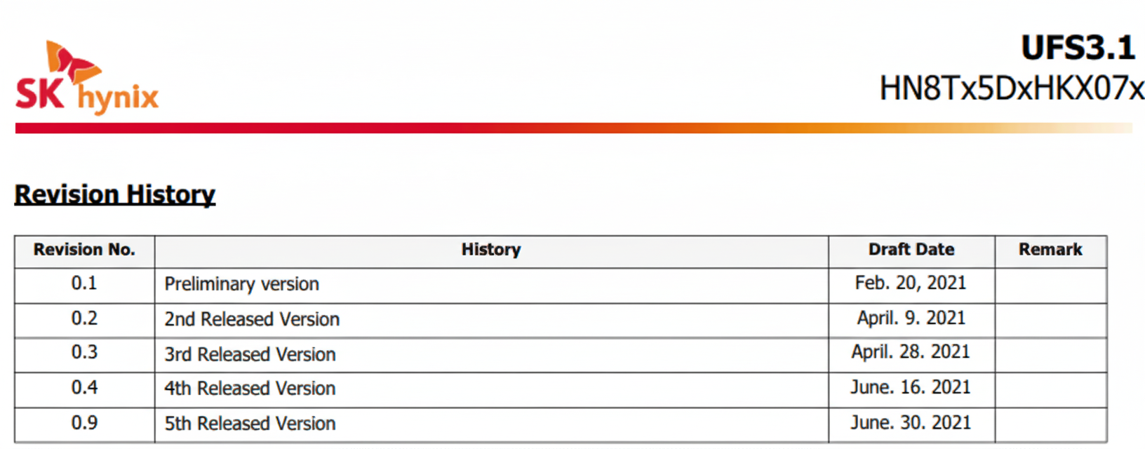
Based on these details, the HN8T25DEHKX077 likely entered production no earlier than the second half of 2021.