Key points
- Technical comparison between NAND Flash and NOR Flash
- Detailed comparison of memory cell structures
- Latest market share and revenue context for NAND and NOR Flash
- Fundamental operating principles
Overview
NOR Flash and NAND Flash are the two main non-volatile flash memory technologies on the market, but many engineers still have difficulty distinguishing them. Below is a technical comparison intended to clarify their differences and applications.
Market context
Recent revenue and market share data indicate which suppliers currently lead the flash market. This information is useful for keeping up with market trends and for component selection in design.
Basic distinctions
Flash memory generally comes in two families: NAND and NOR.
- NAND: Primarily used for data storage. NAND devices offer higher capacity (commonly up to multiple gigabits) and read operations are typically block-oriented, for example reading 512 bytes per transfer. NAND-based flash is cost-effective per bit.
- NOR: Often used for storing program code, also called code flash, because a microprocessor can execute code directly from NOR. NOR devices support random-access memory-like reads and are optimized for fast read performance, but their densities and capacities are typically lower than NAND.
- Because code cannot be executed directly from most NAND devices, many development boards that use NAND also include a small NOR device to hold boot code.
A compact comparison of the important characteristics of NAND and NOR Flash is shown below.
Key flash concepts
- Flash is a non-volatile memory technology. The storage cell is based on a MOSFET with a floating gate that stores charge. By contrast, volatile memories lose data when power is removed, for example older SD RAM or modern DDR3 and DDR4.
- SLC vs MLC: NAND memory cells can be implemented as SLC (single-level cell, storing one bit per cell) or MLC (multi-level cell, storing multiple bits per cell, e.g., two or more bits).
- Most write operations require an erase cycle before programming.
To aid understanding, the following diagram compares the smallest unit structures of various memory types.
Operating principle
Explaining flash operation requires some quantum concepts. Classical physics treats barrier crossing as deterministic with a threshold energy: particles below the threshold cannot cross, while particles above can. In quantum mechanics, even particles with energy below the barrier may tunnel through with a small probability, a phenomenon known as quantum tunneling.
As devices scale down, quantum effects become more significant. Flash erase and program operations rely on tunneling currents that move charge into or out of the floating gate. For NAND devices, erase and program operations use tunneling through the insulating layer between the floating gate and the silicon substrate to charge or discharge the floating gate. NOR devices also use tunneling for erase operations, while programming is typically achieved via hot-electron injection from the channel to the floating gate.
Physically, a flash cell is a three-terminal device with source, drain, and gate. An insulating oxide separates the control gate from the floating gate to prevent charge leakage, allowing stored charge to be retained like liquid in a sealed bottle until intentionally changed by programming or erasing.
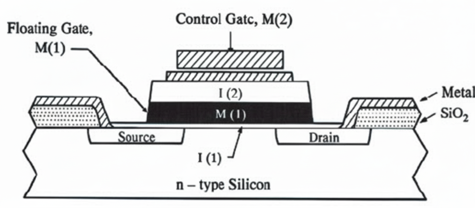
The insulated floating gate is the core element that enables NAND and NOR to store charge.
Summary
- NAND and NOR Flash are common non-volatile memories with different trade-offs in capacity, read/write performance, and cost.
- NAND Flash is suitable for high-capacity data storage because of its higher density and lower cost per bit. It typically has slower random read performance but supports efficient block erase and program operations. NAND is commonly used for storing large files such as multimedia.
- NOR Flash provides faster random read performance and high reliability, making it well suited for storing executable code. NOR allows in-place code execution, which is useful in many embedded systems, though it usually comes at a higher cost per bit.
- Device selection should be based on application requirements: choose NAND for large, low-cost data storage and NOR for fast random reads and in-place code execution.
Practical guidance for learning and using NAND and NOR Flash
First, understand the fundamental operation of NAND and NOR Flash, including their internal structures, operating principles, and read/write differences. This knowledge helps optimize system design and troubleshoot issues.
Second, plan and design hardware carefully to ensure performance and reliability. Consider PCB layout, signal integrity, and power management. Ensure wiring and connections meet design rules and take measures to reduce interference and noise.
Finally, collaborate closely with software engineers during hardware development to ensure compatibility and smooth integration between hardware and firmware, which reduces defects and improves overall system performance.