Key points
- Provides reference circuits for commonly used flash from Huawei, Samsung, and Intel.
- Explains 2-bit and 4-bit NAND flash operation with reference to device datasheets.
- Summarizes debugging approaches and shares practical debugging experience.
- Introduces recent developments in 3D XPoint technology.
2. 2-bit and 4-bit NAND flash configurations
Another commonly used application is the 2-bit or 4-bit NAND flash interface. Hardware engineers selecting devices will see an option such as X1/X2/X4 to choose the number of I/O bits. The circuit topology differs slightly depending on that selection, as shown below.
The diagram shows that several pins are reused, and by combining MISO and MISO signals the data lines D0, D1, D2, and D3 are formed. Details are available in the device specification.
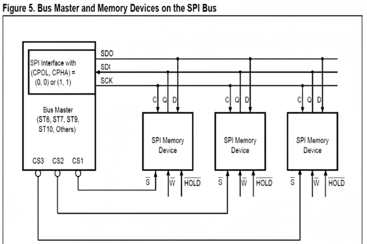
3. Multiple SPI flash chips on one bus
A common implementation is multiple SPI flash chips connected to the CPU via separate chip-select signals. This topology uses separate chip-select lines so multiple SPI flashes can share the same SPI bus.
Debugging experience
Here is a practical debugging case from early development of a motherboard SPI flash.
- When verifying a new SPI flash on the mainboard, the externally connected ROM chip did not operate after soldering, although the soldering appeared correct.
After repeated checks, the main system was found to use 1.8 V supply, while the SPI ROM required 3.3 V. Using a 25XX series chip required a level-shift circuit. As an alternative, replacing the device with a Winbond W25Q32XX 1.8 V part resolved the issue and the system worked.
New technology: 3D XPoint
3D XPoint is a non-volatile memory technology introduced after mainstream NAND flash. It targets lower latency and higher endurance compared with NAND. Key characteristics reported for 3D XPoint include:
- Significantly lower latency than NAND.
- Manufacturing cost stated to be lower than DRAM in some claims.
- Higher write endurance than typical NAND devices.
- Higher density when stacking cells in three dimensions.
3D XPoint uses resistance-based memory cells rather than charge-based floating gates. NAND relies on a floating gate to store charge and represent bits, while 3D XPoint distinguishes states by changing the resistance level of the storage cell. The storage cells can be stacked in 3D to increase density, aiming to combine NAND-like capacity with DRAM-like performance and improved endurance.
NAND and NOR flash operation and debugging notes
NAND flash operations include erase and program. The erase unit is the block, while the program unit is the page. Because a page is much smaller than a block, NAND flash read and write speeds are relatively high, but erase operations are slower and occur at block granularity.
NOR flash operations also include erase and program, but both operations can be performed at bit level. NOR flash read speed is typically faster than NAND, but bit-level erase and program operations are slower, making NOR erase and program slower than NAND in many cases.
When using NAND or NOR flash, pay attention to operation granularity, operation speeds, address mapping, capacity, interface type, and other parameters. Implement bad-block management and data protection. Bad blocks can be identified during manufacturing tests and recorded. Data protection should include backups and checksums where applicable.
Hardware design must also consider power supply and clock circuit requirements to ensure correct flash operation. Software-level debugging and optimization are also required to ensure program correctness and performance.