Introduction
During a hardware interview, I saw a candidate list AMD work or internship experience and familiarity with CPU and memory. I then asked them to draw basic RAM and DRAM cells and briefly describe their operating principles and characteristics, but they could not.
Many people cannot draw these two basic cells, so they cannot claim deep familiarity with CPU and memory. A thorough treatment of both topics is complex, so this article focuses on the basic circuits and operating principles of SRAM to help with comprehension.
Basic Cells: SRAM and DRAM
Below are the basic cell circuits for SRAM and DRAM.
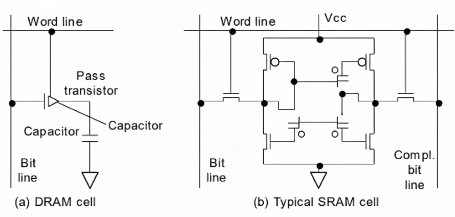
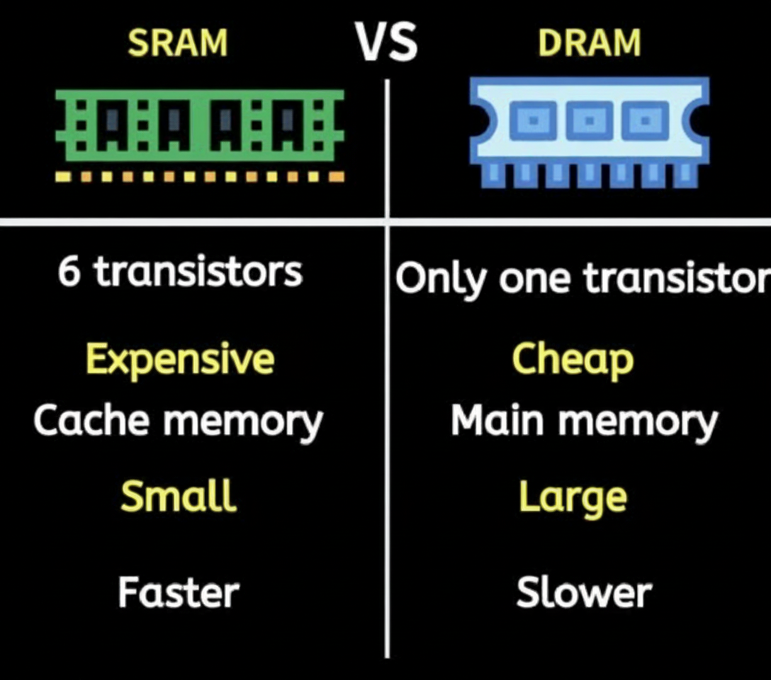
The most obvious difference is that the SRAM structure is much more complex than DRAM, which makes SRAM more expensive. Key differences include:
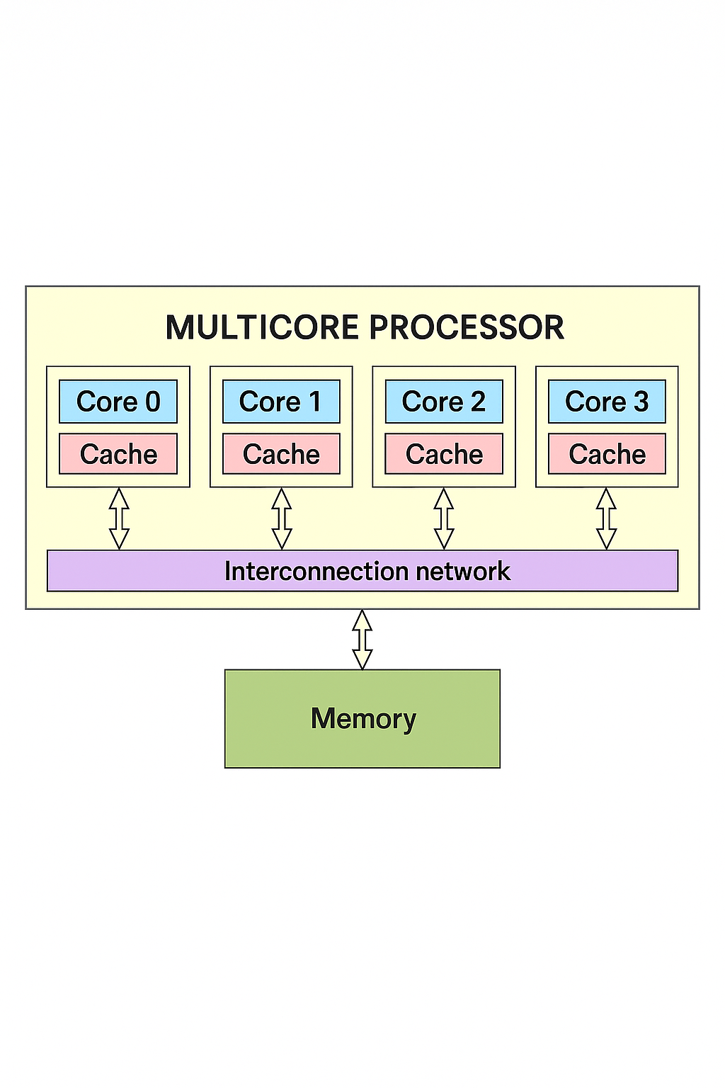
In simple terms, the CPU handles computation and processing, while memory handles data exchange. An analogy is: the CPU is the engineer, main memory is the workbench for items that need immediate processing, and the hard drive is a cabinet for long-term storage.
There are two basic memory types: SRAM and DRAM. Understanding these concepts and their circuit principles is important for studying CPU architecture and DDR memory.
DRAM is dynamic random-access memory, and SRAM is static random-access memory. What does dynamic versus static mean? Static RAM uses a flip-flop structure such as a D flip-flop to store bits, so written data does not require periodic refresh; this is why it is called static. The controller design is relatively simple, and SRAM access is much faster than DRAM, making it suitable for high-speed applications like CPU caches.
DRAM stores data as charge on a capacitor. Because the capacitor leaks charge over time, the data must be periodically refreshed to maintain integrity. DRAM is commonly used for main memory in phones and computers.
Level 1: A D Flip-Flop as the Simplest SRAM Cell
Start from basic digital circuits. A fundamental and direct view is that the simplest SRAM cell can be seen as a D flip-flop. A D flip-flop is a basic element in digital circuits.
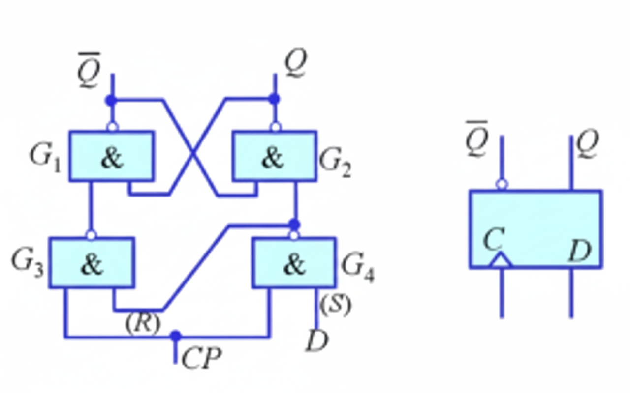
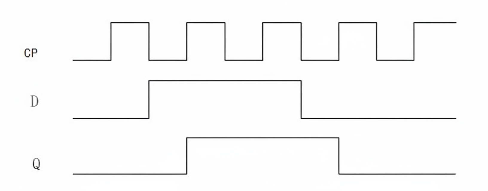
A 1-bit SRAM cell's core circuit is a D flip-flop. With power applied, the D flip-flop stores data without refresh. A flip-flop has memory and two stable states. The D flip-flop characteristic equation is Q(n+1) = D, which stores the previous input state. Starting from an RS flip-flop and writing a truth table helps to understand this. The timing waveform is shown below.
Level 2: A Simple SRAM from Four Transistors
At the transistor level, a simple SRAM cell can be built from four NMOS transistors and two resistors.
Circuit analysis
The cell is symmetric. Aside from Q1 and Q2, which form the storage element, Q1 and Q2 are pass transistors that connect or disconnect the storage node to the peripheral circuitry during read/write operations.
Access to the cell is controlled by the word line WL. When WL is high, the pass transistors conduct and the cell connects to the bit lines BL and BL#. During reads, the cell content is transferred to the bit lines; during writes, the peripheral circuits drive BL and BL# and WL enables writing into the cell.
Level 3: The 6-Transistor SRAM Cell
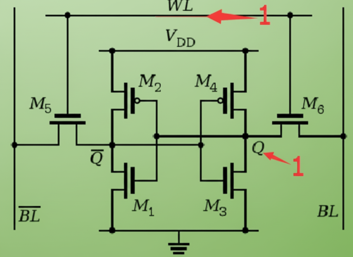
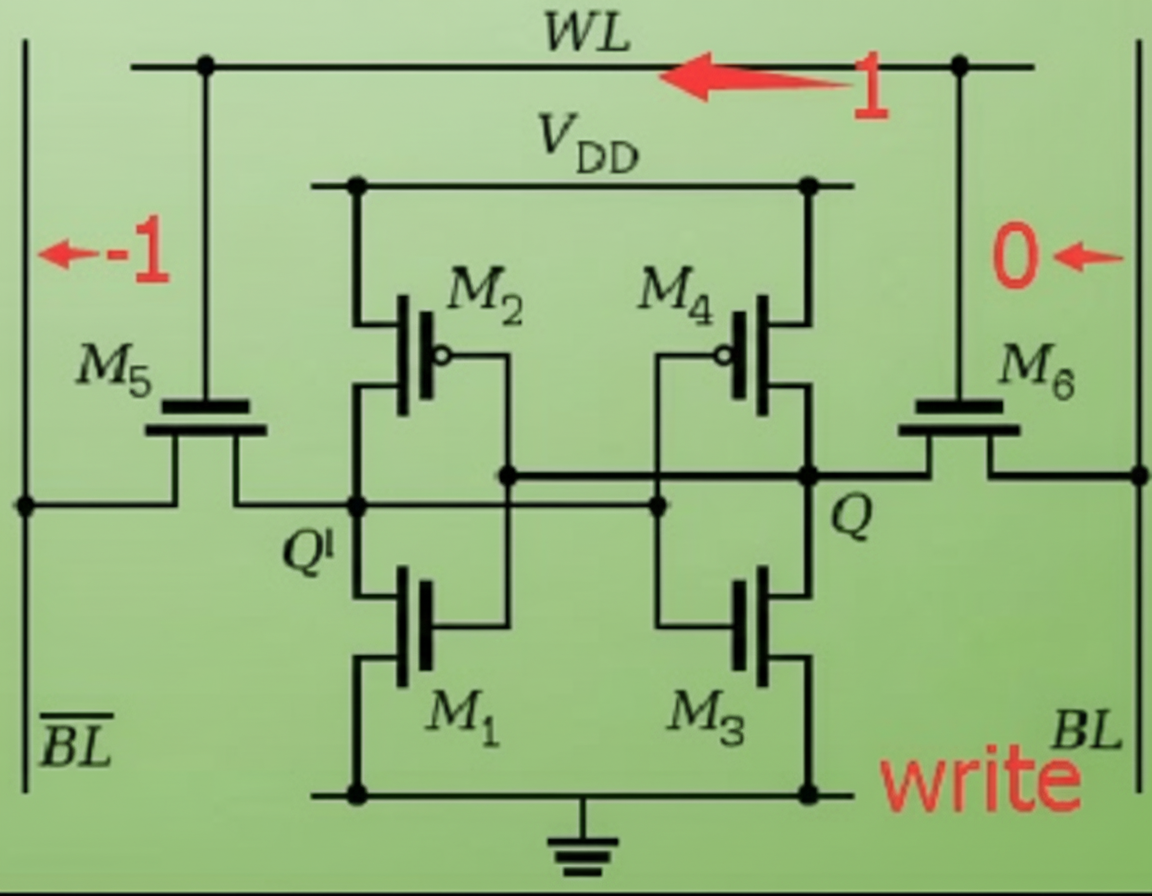
From an IC manufacturing perspective, most SRAM cells use six transistors. Compared with the four-transistor implementation, the two pull-up devices are PMOS transistors. Each bit is stored in two cross-coupled inverters formed by M1, M2, M3, and M4. Two additional transistors, M5 and M6, act as access switches to the bit lines for read and write.
An SRAM cell has two stable states, representing 0 and 1. The cell consists of two CMOS inverters whose inputs and outputs are cross-coupled: the output of the first inverter feeds the input of the second, and the output of the second feeds the input of the first. This cross-coupling locks the outputs and preserves one bit of data. Simplified diagrams are shown below.
Detailed circuit analysis
The basic SRAM cell has three states: standby, read, and write.
Standby
If WL is not asserted (WL is low), transistors M5 and M6 are off, isolating the storage node from the bit lines. The inverters formed by M1–M4 maintain their state.
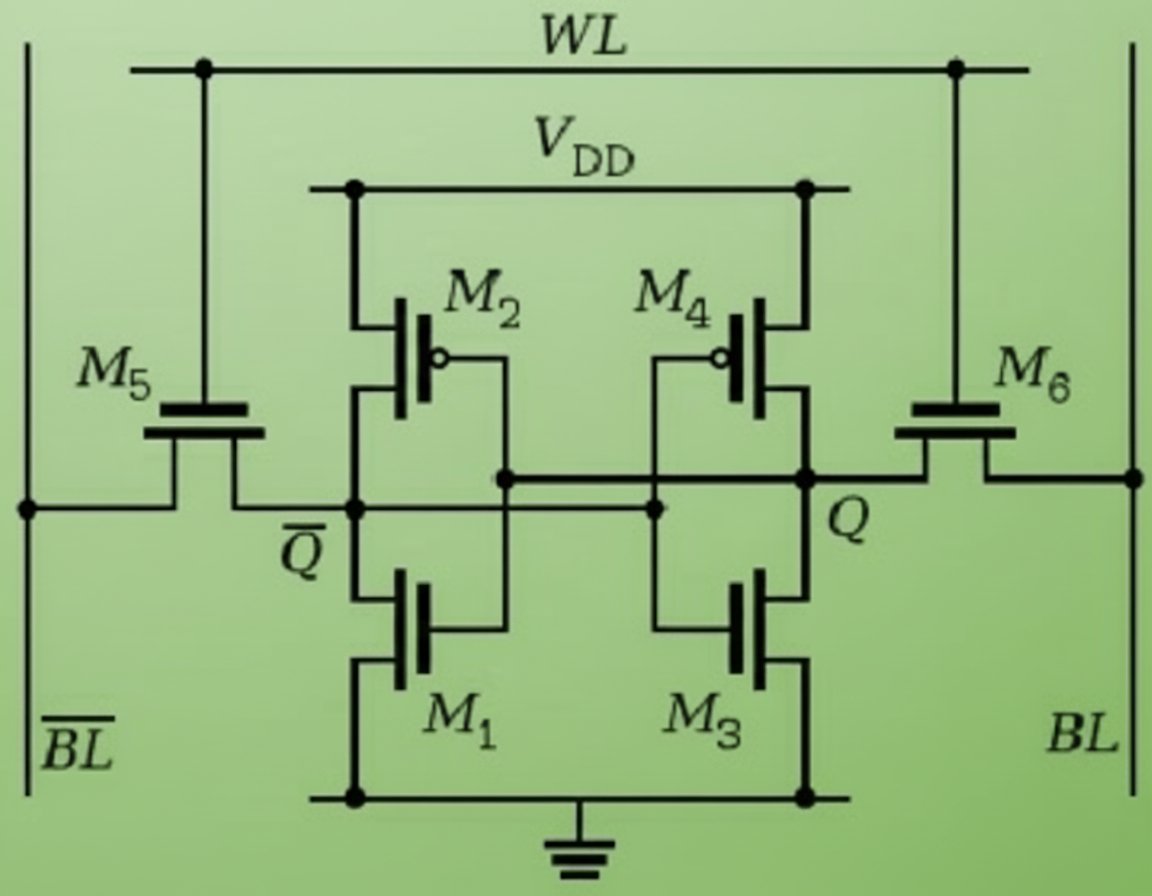
Read
Assume the stored value is 1, so node Q is high. At the start of a read cycle, both bit lines BL and BL# are precharged high. WL is then asserted, turning on M5 and M6 and connecting the cell to the bit lines.
The cell causes a small differential change on the bit lines. The storage node drives one bit line slightly toward its stored level while the other is discharged slightly, and the sense amplifier detects the small difference between BL and BL# to determine the stored bit.
Write
To write, the new value is driven onto BL and BL#. For example, to write 0, set BL to 0 and BL# to 1, then assert WL. The bit lines force the cross-coupled inverters into the new state, completing the write.
Summary
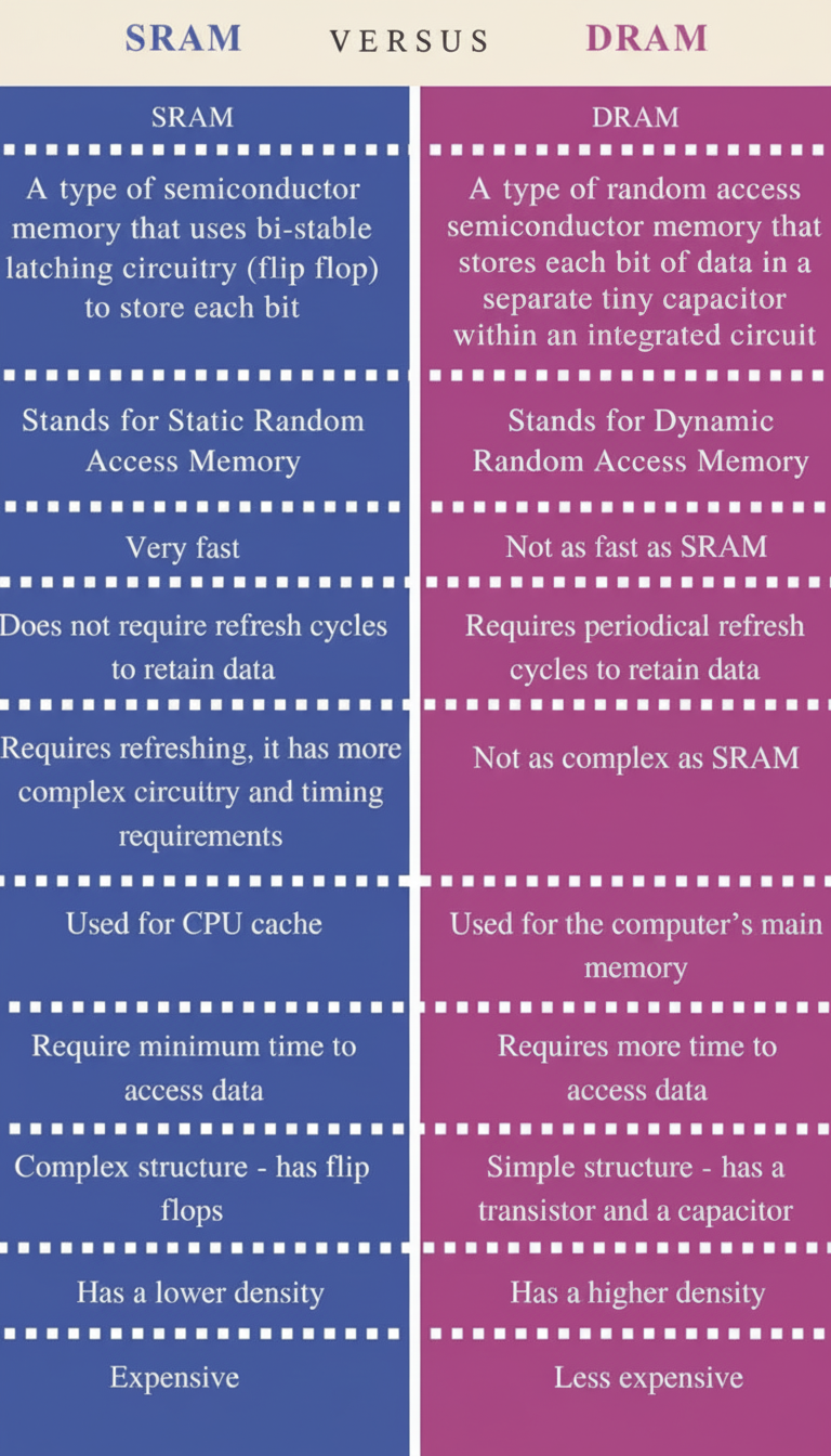
SRAM and DRAM differ in operating principle and storage method. SRAM uses flip-flops to store data, providing faster access at the cost of lower density. DRAM uses capacitors to store charge, offering higher density but slower access and requiring periodic refresh. Choosing between them depends on application requirements.