Overview of FSMC
FSMC stands for flexible static memory controller. It can connect to synchronous or asynchronous memories and 16-bit PC card memories. The FSMC in STM32F4 supports devices including RAM, NAND flash, NOR flash, and PSRAM.
Typical SRAM control signals include address lines (A18..A0), data lines (D15..D0), write enable (WE), output enable (OE), and chip select (CS). If byte control is supported, UB/LB signals are also present.
LCD signals include register select (RS), data lines (D15..D0), write (WE), read (OE), chip select (CS), reset (RST), and backlight (BL).
Excluding RST and BL, the control signals for both devices are very similar. The difference is that SRAM uses address lines (A18..A0) while the LCD uses an RS signal. Functionally both determine which storage location is accessed. If SRAM had only one address line A0, it would provide two addressable locations; similarly, LCD RS=0/1 selects two spaces (command register vs GRAM in the ILI9341). By treating RS as an address line, the LCD behaves like SRAM. In this design RS is tied to address line A6, so A6=0 addresses the ILI9341 registers and A6=1 addresses GRAM.
STM32F4xx FSMC supports 8/16/32-bit data widths. The LCD in this project is 16-bit wide, so a 16-bit data width must be selected. FSMC maps external peripherals into the AHB address space so they can be accessed like internal peripherals. Accessing the mapped AHB addresses operates the external device as if it were internal.
FSMC Memory Regions
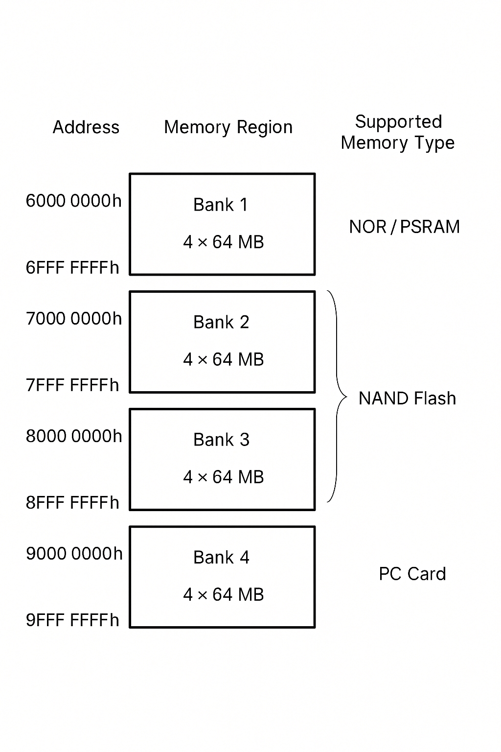
FSMC external memory is divided into four fixed-size regions, each 256 MB.
- Region 1 can connect up to four NOR Flash or PSRAM devices. It is subdivided into four NOR/PSRAM subregions with four dedicated chip-select signals.
- Regions 2 and 3 connect NAND Flash devices (one device per region).
- Region 4 connects PC card devices.
The memory type for each region is defined by the configuration registers.
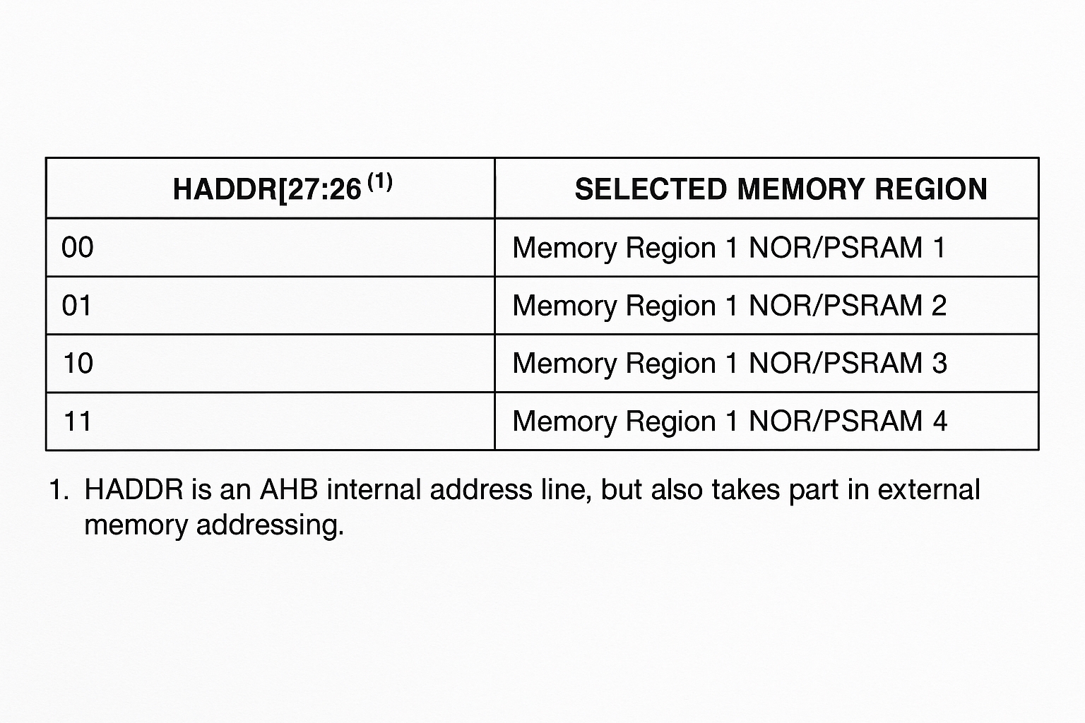
Bank1's 256 MB space is addressed by 28 address lines (HADDR[27:0]). HADDR is an internal AHB byte address. HADDR[25:0] comes from external FSMC_A[25:0], while HADDR[27:26] select the four regions.
NOR/PSRAM Region Selection
Since the LCD chip-select is connected to FSMC_NE4, the base address for the LCD region is 0x60000000 + 0xC000000 = 0x6C000000. The LCD RS is connected to address A6 and no other address lines are used, so other address lines may be set arbitrarily.
HADDR[25:0] contains the external memory address. Because HADDR is a byte address while the memory is word-addressable, the actual internal AHB address depends on the memory data width. The mapping varies with data width.
The LCD is configured for 16-bit data width, so internal address offsets are twice the external address values. If FSMC_A has value x, the mapped internal address is 0x6C000000 + 2*x. Because only A6 (FSMC_A[6]) is used, when that bit is 0 and others are 0, FSMC_A = 0 and the AHB address is 0x6C000000. When FSMC_A[6] = 1 and others are 0, FSMC_A = 0x40 and the AHB address becomes 0x6C000000 + 2*0x40 = 0x6C000080. With these addresses, the external LCD can be accessed like an internal peripheral.
For convenience, the addresses are defined with macros.
// All unused address lines set to 0 (note: any value is acceptable; 0 is used here)
#define   LCD_CMD_ADD      (volatile u16 *)0X6C000000
#define   LCD_DATA_ADD     (volatile u16 *)(0X6C000000 + 0X80)
To simplify access, the address macros can be dereferenced with another pair of macros.
#define   LCD_CMD          *LCD_CMD_ADD
#define   LCD_DATA         *LCD_DATA_ADD
With these macros, writing a command is as simple as assigning to LCD_CMD, and writing data is assigning to LCD_DATA.
Timing Requirements
With the LCD mapped into the AHB address space, ILI9341 registers and GRAM can be accessed, but correct timing is required. Programmable SRAM timing parameters are shown below.
Because ILI9341 read and write speeds differ significantly, asynchronous mode A is used to optimize both. In this mode, the three parameters to focus on are address setup time, address hold time, and data setup time.
ILI9341 8080-II Read/Write Timing
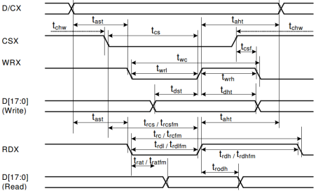
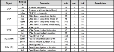
From the timing table: write control pulse high duration twrh < 15 ns (HCLK=168 MHz, so twrh < 3 HCLK); write control pulse low duration twrl < 15 ns (twrl < 3 HCLK). Read GRAM control pulse high duration trdhfm < 90 ns (< 15 HCLK); read GRAM control pulse low duration trdlfm < 355 ns (< 60 HCLK). Read ID control pulse high trdh < 90 ns (< 15 HCLK); read ID control pulse low trdl < 45 ns (< 8 HCLK).
Writes are much faster than reads. To ensure read GRAM and read ID can share a read timing, the read control low time trd should be at least 60 HCLK. To exploit fast writes, separate read and write timing configurations are used.
FSMC Mode A Read/Write Timing
In read timing, ADDSET corresponds to read control high time and should be 90 ns (15 HCLK). DATAST corresponds to read control low time and should be 355 ns (60 HCLK). In write timing, ADDSET corresponds to write control high and should be 15 ns (3 HCLK). DATAST corresponds to write control low and should be 15 ns (3 HCLK).
With these timing parameters, FSMC registers can be configured accordingly.
FSMC Register Overview
Brief description of relevant registers:
SRAM/NOR-Flash chip-select control registers 1..4 (FSMC_BCR1..4)
Key bits:
- bit19: burst write enable. For PSRAM this enables synchronous burst protocol on write. For LCD asynchronous operation is used, so set 0.
- bit15: NWAIT during asynchronous transfer. Controls consideration of NWAIT in async protocol. Default is 0; here NWAIT is not used.
- bit14: extended mode enable (EXTMOD). When set, write timing from FSMC_BWTR is used so read and write can have different timings. For Mode A extended mode is enabled.
- bit13: NWAIT enable, not needed here.
- bit12: write enable. Set to allow writes to the region.
- bit11: NWAIT timing configuration, not used here.
- bit10: wrap burst support, not used.
- bit9: NWAIT polarity, not needed.
- bit8: burst enable for read, not needed for async mode.
- bit6: NOR FLASH enable. Since the LCD is treated as SRAM, disable this bit.
- bit[5:4]: data bus width. 00 = 8-bit, 01 = 16-bit. Set to 16-bit.
- bit[3:2]: memory type. 00 = SRAM/ROM, 01 = PSRAM, 10 = NOR FLASH. Configure as SRAM.
- bit1: address/data multiplex enable, not relevant here.
- bit0: memory region enable. Must be enabled.
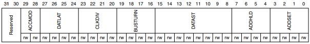
SRAM/NOR-Flash chip-select timing registers 1..4 (FSMC_BTR1..4)
Key fields:
- bit[29:28]: access mode. 00 = Mode A; 01 = Mode B; 10 = Mode C; 11 = Mode D. Choose Mode A.
- bit[27:24]: DATLAT for synchronous burst NOR FLASH, not used.
- bit[23:20]: CLKDIV, not relevant for async mode.
- bit[15:8]: DATST, data phase duration for read. Set to 60 HCLK.
- bit[7:4]: ADDHLD, address hold time, not relevant in async mode.
- bit[3:0]: ADDSET, address setup time. Set to 15 HCLK for read.
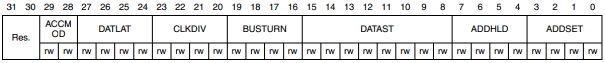
SRAM/NOR-Flash write timing registers 1..4 (FSMC_BWTR1..4)
Key fields:
- bit[29:28]: access mode, set to Mode A.
- bit[15:8]: DATST, data phase duration for write. Set to 3 HCLK.
- bit[3:0]: ADDSET, address setup for write. Set to 3 HCLK.
After configuring the GPIO pins for FSMC alternate function and setting the FSMC registers as analyzed, FSMC will provide the required timing to the LCD.
FSMC Register Mapping
In stm32f4xx.h the FSMC structure is defined as:
typedef struct{
    __IO uint32_t BTCR[8];    /*!< NOR/PSRAM chip-select control register(BCR) and chip-select timing register(BTR) */
} FSMC_Bank1_TypeDef;
#define   FSMC_Bank1          ((FSMC_Bank1_TypeDef *) FSMC_Bank1_R_BASE)
The structure contains an 8-element array. Due to contiguous array allocation, BTCR[0] maps to FSMC_BCR1, BTCR[1] to FSMC_BTR1, BTCR[2] to FSMC_BCR2, BTCR[3] to FSMC_BTR2, BTCR[4] to FSMC_BCR3, BTCR[5] to FSMC_BTR3, BTCR[6] to FSMC_BCR4, and BTCR[7] to FSMC_BTR4.
The write timing registers are arranged similarly with gaps to match register address spacing.
Configuring FSMC
static void ILI9341_GpioInit(){
  // 1. Enable clocks for PB/PD/PE/PF/PG
  RCC->AHB1ENR |= 1<<1 | 0xF<<3;

  // 2. Backlight pin: general push-pull output
  // port config (PB15)
  GPIOB->MODER &= ~(0X3<<30);
  GPIOB->MODER |= 1<<30;          // general output
  GPIOB->OTYPER &= ~(1<<15);      // push-pull
  GPIOB->OSPEEDR |= 0X3<<30;
  GPIOB->PUPDR &= ~(0X3<<30);     // no pull-up/pull-down

  // All other pins multiplexed to FSMC
  /*
    LCD_CS:PG12
    RS:PF12 => FSMC_A[6]
    WR:PD5
    RD:PD4
    D0-D1:PD14/PD15
    D2-D3:PD0/PD1
    D4-D12:PE7-PE15
    D13-D15:PD8-PD10
  */

  // 2. PD (configured for alternate function)
  GPIOD->MODER &= ~(0XF<<0 | 0XF<<8 | 0X3F<<16 | 0xf<<28);
  GPIOD->MODER |=  0X0a<<0 | 0x0a<<8 | 0x2a<<16 | 0xa<<28;        // PD port alternate function
  GPIOD->OTYPER &= ~(0X3<<0 | 0X3<<4 | 0X7<<8 | 0X3<<14);         // push-pull
  GPIOD->OSPEEDR  |= (0XF<<0 | 0XF<<8 | 0X3F<<16 | 0xf<<28);      // speed 100 MHz
  GPIOD->PUPDR     &= ~(0XF<<0 | 0XF<<8 | 0X3F<<16 | 0xf<<28);    // no pull-up/pull-down

  // PE port configuration
  GPIOE->MODER    &= 0X00003FFF;
  GPIOE->MODER    |= 0Xaaaa8000;        // PE alternate function
  GPIOE->OTYPER   &= 0X007F;            // PE7-15 push-pull
  GPIOE->OSPEEDR  |= 0XFFFC000;         // PE7-15 speed 100 MHz
  GPIOE->PUPDR    &= 0X00003FFF;        // PE7-15 no pull-up/pull-down

  // PF12
  GPIOF->MODER    &= ~(0X3<<24);
  GPIOF->MODER    |= 2<<24;
  GPIOF->OTYPER   &= ~(1<<12);          // push-pull
  GPIOF->OSPEEDR  |= 0X3<<24;           // 100 MHz
  GPIOF->PUPDR    &= ~(0X3<<24);        // no pull-up/pull-down

  // PG12
  GPIOG->MODER    &= ~(0X3<<24);
  GPIOG->MODER    |= 2<<24;
  GPIOG->OTYPER   &= ~(1<<12);          // push-pull
  GPIOG->OSPEEDR  |= 0X3<<24;           // 100 MHz
  GPIOG->PUPDR    &= ~(0X3<<24);        // no pull-up/pull-down

  // Select alternate function: FSMC
  // PD:
  GPIOD->AFR[0] &= 0XFF00FF00;
  GPIOD->AFR[0] |= 0x00cc00cc;          // PD0/1/4/5 alternate function FSMC
  GPIOD->AFR[1] &= 0X00FFF000;
  GPIOD->AFR[1] |= 0XCC000CCC;          // PD8/9/10/14/15 alternate function FSMC

  // PE:
  GPIOE->AFR[0]  &= 0X0FFFFFFF;
  GPIOE->AFR[0] |= 0XC0000000;          // PE7 alternate function FSMC
  GPIOE->AFR[1] &= 0x00000000;
  GPIOE->AFR[1] |= 0XCCCCCCCC;          // PE8-15 alternate function

  // PF:
  GPIOF->AFR[1] &= 0xfff0ffff;
  GPIOF->AFR[1] |= 0X000C0000;          // PF12 alternate function FSMC

  // PG:
  GPIOG->AFR[1] &= 0xfff0ffff;
  GPIOG->AFR[1] |= 0X000C0000;          // PG12 alternate function FSMC

  // 3. Enable FSMC clock
  RCC->AHB3ENR |= 1<<0;

  // 4. Configure FSMC registers
  // BCR4
  FSMC_Bank1->BTCR[6] &= ~(1<<19);      // Always operate in asynchronous mode
  FSMC_Bank1->BTCR[6] &= ~(1<<15);      // Do not consider wait signal
  FSMC_Bank1->BTCR[6] |= 1<<14;         // Enable extended mode to separate read/write timing
  FSMC_Bank1->BTCR[6] &= ~(1<<13);      // Disable NWAIT
  FSMC_Bank1->BTCR[6] |= 1<<12;         // Enable write operations
  FSMC_Bank1->BTCR[6] &= ~(0x3<<4);
  FSMC_Bank1->BTCR[6] |= 1<<4;          // 16-bit data width
  FSMC_Bank1->BTCR[6] &= ~(0x3<<2);     // Memory type: SRAM

  // BTR4 (read timing)
  FSMC_Bank1->BTCR[7]  &= ~(0x3<<28);   // Mode A
  FSMC_Bank1->BTCR[7] |= 0xf<<16;       // Bus turnaround default
  FSMC_Bank1->BTCR[7] &= 0xffff00ff;
  FSMC_Bank1->BTCR[7] |= 60<<8;         // DATAST = 60 HCLK
  FSMC_Bank1->BTCR[7] |= 0xf<<0;        // ADDSET = 15 HCLK

  // BWTR (write timing)
  FSMC_Bank1E->BWTR[6] = 0;
  FSMC_Bank1E->BWTR[6] &= ~(0x3<<28);   // Mode A
  FSMC_Bank1E->BWTR[6] |= 0xf<<16;      // Bus turnaround default
  FSMC_Bank1E->BWTR[6] |= 3<<8;         // DATAST = 3 HCLK
  FSMC_Bank1E->BWTR[6] |= 3<<0;         // ADDSET = 3 HCLK

  // Enable memory bank
  FSMC_Bank1->BTCR[6] |= 1<<0;
  GPIOB->BSRRH  = 0X1<<15;              // Turn off backlight
}
Results and Notes
Replacing GPIO-based 8080 timing simulation with FSMC initialization and mapped accesses significantly improves screen refresh speed. While hardware-based FSMC is faster than a naive software-timed GPIO implementation, optimized GPIO timing using a logic analyzer to tune delays can approach FSMC performance. Interested readers can experiment comparing both approaches.