Overview
The SRAM used in this example is the IS62WV51216, a high-speed 8M-bit static SRAM. It is manufactured using ISSI (Integrated Silicon Solution, Inc.) high-performance CMOS technology and is organized as 512K words of 16 bits. The device offers high performance and low power consumption. To facilitate memory expansion, it provides two chip-select pins and includes two byte control signals, UB and LB, enabling byte or word access. IS62WV51216 supports 45ns/55ns access times and, being fully static, does not require an external clock or refresh.
IS62WV51216 functional block diagram
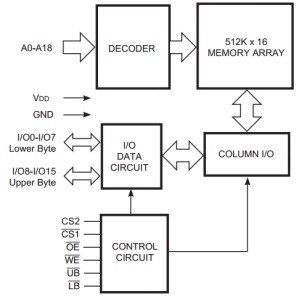
The IS62WV51216 consists of an address decoder, data I/O, control logic, and the memory array. The address decoder maps the 19 input address lines to internal memory addresses. The data I/O provides the data path between the SRAM and the main controller. Access can be byte-wide or word-wide; byte access improves compatibility with 8-bit hosts. The control logic includes read/write control signals and byte-enable and chip-select pins.
Hardware connection
In the hardware connection, the SRAM is connected to the STM32F4 via the FSMC interface. The SRAM chip-select CE is tied to FSMC NE3, so the SRAM occupies Bank1, region 3 and is mapped starting at 0x68000000. Because the SRAM has a 16-bit data bus, the FSMC data width is configured as 16 bits to improve throughput.
When an FSMC interface address is mapped into the AHB address space, each FSMC address corresponds to two AHB byte addresses, reflecting the u16 data width. When the CPU accesses byte addresses in AHB space, accessing the lower byte of a word corresponds to the SRAM low byte, and accessing the higher byte corresponds to the SRAM high byte. The UB and LB pins allow byte-level access to the same FSMC address. Therefore, with UB and LB, external devices on the FSMC interface can be accessed by byte or by word.
SRAM initialization function
void SRAM_Init(){
  // 1. Enable clocks for PD/PE/PF/PG
  RCC->AHB1ENR |= 0xF << 3;
  // Configure all related pins for FSMC alternate function
  /*
    LCD_CS: PG12
    RS: PF12 => FSMC_A[6]
    WR: PD5
    RD: PD4
    D0-D1: PD14/PD15
    D2-D3: PD0/PD1
    D4-D12: PE7-PE15
    D13-D15: PD8-PD10
  */
  // 2. Configure GPIOD (set to alternate function)
  GPIOD->MODER &= ~(0xF << 0 | 0xF << 8 | 0x3F << 16 | 0xF << 28);
  GPIOD->MODER |=  0x0A << 0 | 0x0A << 8 | 0x2A << 16 | 0x0A << 28;
  // GPIOD alternate function output type
  GPIOD->OTYPER &= ~(0x3 << 0 | 0x3 << 4 | 0x7 << 8 | 0x3 << 14);
  // Push-pull
  GPIOD->OSPEEDR |= (0xF << 0 | 0xF << 8 | 0x3F << 16 | 0xF << 28);
  // Speed 100MHz
  GPIOD->PUPDR &= ~(0xF << 0 | 0xF << 8 | 0x3F << 16 | 0xF << 28);
  // No pull-up/pull-down
  GPIOD->MODER = 0x0F03FFFF;
  // PD11-PD13
  GPIOD->MODER |= 0x0A800000;
  GPIOD->OTYPER &= ~(0x7 << 11);
  GPIOD->OSPEEDR |= 0x3F << 22;
  GPIOD->PUPDR &= ~(0x3F << 22);
  // Configure GPIOE
  GPIOE->MODER &= 0x00003FFF;
  GPIOE->MODER |= 0xAAAA8000;
  // GPIOE alternate function
  GPIOE->OTYPER = 0x007F;
  // PE7-15 push-pull
  GPIOE->OSPEEDR |= 0xFFFC000;
  // PE7-15 speed 100MHz
  GPIOE->PUPDR &= 0x00003FFF;
  // PE7-15 no pull
  GPIOE->MODER = 0xFFFFFFF0;
  GPIOE->MODER |= 0x0000000A;
  // PE0/1 alternate function
  GPIOE->OTYPER &= 0xFFFFFFFC;
  GPIOE->OSPEEDR |= 0x0000000F;
  GPIOE->PUPDR &= 0xFFFFFFF0;
  // PF12 configuration
  GPIOF->MODER &= ~(0x3 << 24);
  GPIOF->MODER |= 2 << 24;
  GPIOF->OTYPER &= ~(1 << 12);
  // Push-pull
  GPIOF->OSPEEDR |= 0x3 << 24;
  // 100MHz
  GPIOF->PUPDR &= ~(0x3 << 24);
  // No pull
  // FSMC_A0~FSMC_A5: PF0~PF5
  // FSMC_A7~FSMC_A9: PF13~PF15
  GPIOF->MODER &= 0x03FFF000;
  GPIOF->MODER |= 0xA8000AAA;
  GPIOF->OTYPER &= ~(0x3F << 0 | 0x7 << 13);
  // Push-pull
  GPIOF->OSPEEDR |= 0xFC000FFF;
  // 100MHz
  GPIOF->PUPDR = 0x03FFF000;
  // No pull
  // PF10
  GPIOG->MODER &= ~(0x3 << 20);
  GPIOG->MODER |= 2 << 20;
  GPIOG->OTYPER &= ~(1 << 10);
  // Push-pull
  GPIOG->OSPEEDR |= 0x3 << 20;
  // 100MHz
  GPIOG->PUPDR &= ~(0x3 << 20);
  // No pull
  // FSMC_A10~FSMC_A15: PG0~PG5
  GPIOG->MODER = 0xFFFFF000;
  GPIOG->MODER |= 0x00000AAA;
  GPIOG->OTYPER &= ~(0x3F << 0);
  // Push-pull
  GPIOG->OSPEEDR |= 0x00000FFF;
  // 100MHz
  GPIOG->PUPDR = 0xFFFFF000;
  // No pull
  // Select alternate function: FSMC
  // AF selection for PD: PD0/1/4/5/8-15
  GPIOD->AFR[0] &= 0xFF00FF00;
  GPIOD->AFR[0] |= 0x00CC00CC;
  // PD0/1/4/5 alternate to FSMC
  GPIOD->AFR[1] = 0;
  GPIOD->AFR[1] |= 0xCCCCCCCC;
  // PD8-15 alternate to FSMC
  // PE:
  GPIOE->AFR[0] &= 0x0FFFFF00;
  GPIOE->AFR[0] |= 0xC00000CC;
  // PE7 alternate to FSMC
  GPIOE->AFR[1] &= 0x00000000;
  GPIOE->AFR[1] |= 0xCCCCCCCC;
  // PE8-15 alternate
  // PF: 0-5 12-15
  GPIOF->AFR[0] &= 0xFF000000;
  GPIOF->AFR[0] |= 0x00CCCCCC;
  // PF0-5 alternate to FSMC
  GPIOF->AFR[1] &= 0x0000FFFF;
  GPIOF->AFR[1] |= 0xCCCC0000;
  // PF12-15 alternate to FSMC
  // PG:0-5 10
  GPIOG->AFR[0] &= 0xFF000000;
  GPIOG->AFR[0] |= 0x00CCCCCC;
  // PG0-5 alternate to FSMC
  GPIOG->AFR[1] &= 0xFFFfF0FF;
  GPIOG->AFR[1] |= 0x00000C00;
  // PG10 alternate to FSMC
  // Configure FSMC
  // 3. Enable FSMC clock
  RCC->AHB3ENR |= 1 << 0;
  // 4. Configure FSMC registers
  // BCR3
  FSMC_Bank1->BTCR[4] &= ~(1 << 19);
  // Always operate in asynchronous mode
  FSMC_Bank1->BTCR[4] &= ~(1 << 15);
  // Do not use wait signal
  FSMC_Bank1->BTCR[4] |= 1 << 14;
  // Enable extended mode: separate read/write timings
  FSMC_Bank1->BTCR[4] &= ~(1 << 13);
  // Disable nWAIT signal
  FSMC_Bank1->BTCR[4] |= 1 << 12;
  // Enable write operations
  FSMC_Bank1->BTCR[4] &= ~(0x3 << 4);
  FSMC_Bank1->BTCR[4] |= 1 << 4;
  // 16-bit data width
  FSMC_Bank1->BTCR[4] &= ~(0x3 << 2);
  // Memory type: SRAM
  // BTR4 (read timing)
  FSMC_Bank1->BTCR[5] &= ~(0x3 << 28);
  // Asynchronous mode A
  FSMC_Bank1->BTCR[5] |= 0xF << 16;
  // Bus turnaround phase is default
  FSMC_Bank1->BTCR[5] &= 0xFFFF00FF;
  FSMC_Bank1->BTCR[5] |= 5 << 8;
  // DATAST = 5 HCLK
  FSMC_Bank1->BTCR[5] |= 0x10 << 0;
  // ADDSET = 10 HCLK
  // BWTR (write timing)
  FSMC_Bank1E->BWTR[4] = 0;
  FSMC_Bank1E->BWTR[4] &= ~(0x3 << 28);
  // Asynchronous mode A
  FSMC_Bank1E->BWTR[4] |= 0xF << 16;
  // Bus turnaround phase default
  FSMC_Bank1E->BWTR[4] |= 8 << 8;
  // DATAST = 3 HCLK
  FSMC_Bank1E->BWTR[4] |= 0 << 0;
  // ADDSET = 3 HCLK
  // Enable the memory bank
  FSMC_Bank1->BTCR[4] |= 1 << 0;
}
Static buffer placement
u16 buf[512] __attribute__((at(SRAM_ADD+0))); // Located at the SRAM start address SRAM_ADD
Placing buffers in external SRAM is useful for large caches, such as UART receive buffers or other large temporary storage.
Main function
#include "usart.h"
#include "stdio.h"
#include "stm32f4xx.h"
#include "stdlib.h"
#include "sram.h"

// Note: SRAM usable address range: 0x68000000 ~ 0x680FFFFF
// When allocating buffers, ensure the allocated space lies within the SRAM range
u16 buf[512] __attribute__((at(SRAM_ADD+0)));

int main()
{
  u32 i = 0;
  Usart1_Init(115200);
  SRAM_Init();

  for(i = 0; i < 512; i++)
    buf[i] = 0;

  for(i = 0; i < 512; i++)
    buf[i] = i;

  while(1)
  {
    for(i = 0; i < 512; i++)
      printf("buf[%d] = %d\r\n", i, buf[i]);
  }
}
After compiling and programming the device, the serial terminal will display the data written into the SRAM.