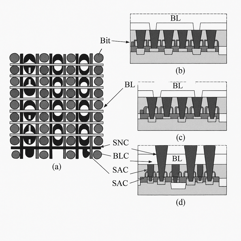
SNC via structure
The diagrams below show the structural details of stacked DRAM storage node related sections. Figure (a) shows the stacked DRAM storage node contact (SNC) structure. The SNC via connects to the two sidewalls of the AA array through an SAC plug. The conductive plug can be formed from polysilicon or tungsten; the choice depends on the technology node.
Typically, before depositing the conductive layer, a silicon nitride layer is deposited and re-etched to form a spacer on the SNC via sidewalls. This spacer prevents a short circuit between the bitline and the conductive plug.
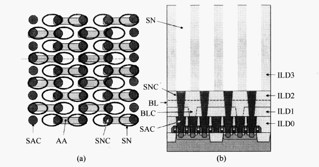
Layout and SN via cross-section
Figure (a) shows the storage node layout. Figure (b) is a cross-section of the SN via along the dashed line in Figure (a). The SN via connects to the SNC plug, and the SNC plug connects to the two sidewalls of the AA array via the SAC plug rather than making a direct connection.
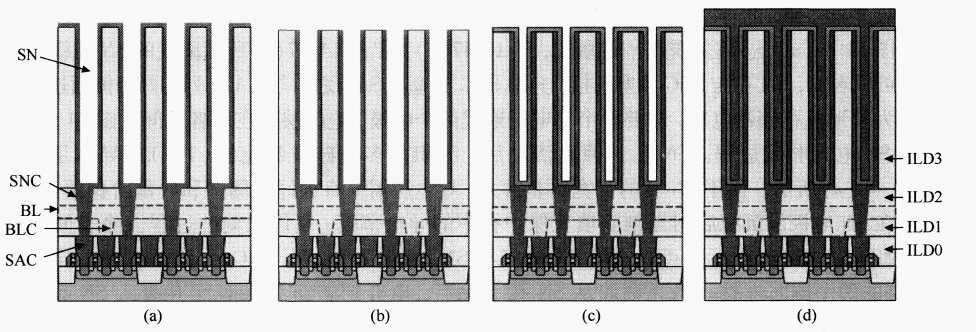
SN capacitor formation process
To form the memory capacitor, two conductive layers are used as the capacitor's top and bottom plates. These conductive layers are connected to the positive and negative terminals of a power supply to form the two electrodes, with a dielectric layer between them serving as the capacitor dielectric. The following describes the SN capacitor formation process.
After SN via etch and clean, a conductor layer such as polysilicon or titanium nitride (TiN) is deposited, as shown in figure (a). Because the SN via has a very high aspect ratio, the conductive layer requires good sidewall and bottom step coverage.
Typically, after depositing the SN electrode layer, photoresist is used to fill and protect the conductive film inside the via. A re-etch process then removes the surface conductive film, as shown in figure (b). The SN electrode connects to the SNC plug, and the SNC plug connects to the two sidewalls of the AA layer through the SAC plug. After the photoresist is removed from the SN via, the dielectric is deposited on the surface and into the SN via, as shown in figure (c).
To achieve the required dielectric characteristics, uniform step coverage on the sidewalls and bottom is necessary; specific process steps are used to ensure this uniformity. Figure (d) shows the ground electrode formed by conductive deposition to complete the SN capacitor. This conductive layer will be removed from the peripheral area in a subsequent lithography step, completing part of the DRAM device process and initiating BEOL interconnect processing.
Reducing SN via aspect ratio and material choices
As the technology node scales, SN via dimensions shrink. To achieve a target SN capacitance (for example around 30 fF) to retain sufficient charge, and if capacitor geometry and dielectric materials remain unchanged, the SN via aspect ratio must increase. Several techniques have been developed to reduce the required aspect ratio.
Using high-k dielectrics can lower the required SN via height and aspect ratio. Earlier stacks used silicon dioxide and silicon nitride, while high-k materials such as aluminum oxide (Al2O3), hafnium dioxide (HfO2), and zirconium dioxide (ZrO2) have been applied to SN capacitors.
Another approach to reduce SN via height is to reduce ILD3 formed after SN electrode creation, which allows ground electrodes to form on both sides of the SN electrode. Polysilicon was widely used as the electrode material in the past; advanced DRAM chips have begun using TiN as the SN electrode. The figure below shows a newer stacked DRAM structure where the transistor array uses a recessed-gate (RG) structure, TiN is used as the SN electrode, ILD3 is recessed, a high-k dielectric layer is used, and a three-metal-layer interconnect ground electrode is employed. The recessed-gate structure helps reduce short-channel effects (SCE) in the NMOS transistor array, which become more severe as feature sizes shrink.