Overview
TSMC is leveraging its advanced process capabilities to develop emerging memory technologies. In recent years, driven by AI, 5G and related trends, memory technologies such as magnetoresistive RAM (MRAM), ferroelectric RAM (FRAM), phase-change RAM (PRAM), and resistive RAM (RRAM) have attracted growing attention.
Why MRAM Is in Focus
MRAM has become a leading candidate among these technologies. It is a non-volatile memory built from magnetoresistive materials, so stored data is retained when power is removed. MRAM offers low energy consumption and fast read/write performance comparable to SRAM and substantially faster than NAND flash, and its density and retention characteristics make it suitable for high-performance applications and, in some cases, as an alternative to DRAM.
The basic MRAM cell is a magnetic tunnel junction. Development is challenging, and current implementations are mainly classified into two types: conventional field-driven MRAM and spin-transfer-torque MRAM (STT-MRAM), which uses a spin-polarized current for switching.
Compared with DRAM, SRAM and NAND flash, which face scaling challenges, MRAM can be scaled further. DRAM process nodes at the 1x nm scale are approaching limits, and NAND flash shifted to 3D structures below 20 nm. MRAM process scaling can potentially advance below 10 nm.
TSMC and ITRI SOT-MRAM Demonstration
TSMC and the Industrial Technology Research Institute (ITRI) in Taiwan recently demonstrated a jointly developed spin-orbit-torque (SOT) MRAM device. The device targets in-memory computing and advanced cache roles. According to the demonstration, the SOT-MRAM is faster than DRAM, retains data after power-off, is intended as a replacement for STT-MRAM, and reduces operating power by a factor of 100 compared with comparable technologies.
STT-MRAM and SOT-MRAM Technical Points
STT-MRAM has long been considered a contender for higher-level caches (L3 and above) and for non-volatile in-memory computing. STT-MRAM switches magnetization by passing a spin-polarized current through a tunnel junction, which generally consumes several times less energy than field-driven conventional MRAM.
SOT-MRAM takes a different approach: switching of the ferromagnetic layer is assisted by spin-orbit torque. This effect arises from a combination of phenomena in the conductor beneath the ferromagnet, notably the spin Hall effect and the Rashba effect. The conductor generates a spin current that influences the adjacent ferromagnet, enabling lower-power switching. SOT-MRAM also benefits from separate write and read circuits, which improves both performance and endurance.
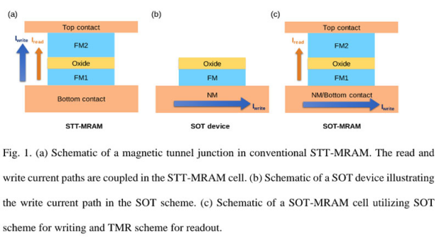
Write and read current paths for two types of MRAM cells. Source: National University of Singapore.
Performance and Use Cases
Dr. Zhang Shiji, head of the Electronics and Photonics Research Laboratory at ITRI, stated that the cell provides low-power and high-speed operation, with speeds up to 10 ns. Implementing in-memory computing circuits can further improve overall computational performance. Potential application areas include high-performance computing (HPC), AI accelerators, and automotive SoCs.
Compared with conventional DRAM latency, which can reach 100 ns or more, SOT-MRAM latency as low as 10 ns is closer to SRAM (on the order of 2 ns). By contrast, 3D NAND TLC typically exhibits latencies in the 50 to 100 microsecond range, so SOT-MRAM is substantially faster than NAND flash. Although SOT-MRAM is not yet ready for immediate integration into processors and controllers, it may become important for efficient in-memory computing and self-powered devices.
Industry Activity
Major foundries and memory developers are investing in these technologies. Notable companies include Intel and Samsung.
Intel has been active in MRAM development using FinFET-based 22 nm processes. In late 2018, Intel disclosed STT-MRAM research based on a 22 nm FinFET process and indicated readiness for production at that node.
Samsung began MRAM research in 2002 and STT-MRAM work in 2005. In 2019, Samsung released a 1 Gb embedded STT-MRAM product using the 28FDS process. The eMRAM implementation reported high yields above 90% while meeting read/write requirements and 10-year data retention targets, with endurance up to 1E10 cycles.
In late 2019, Mentor announced IC test solutions for Arm-based eMRAM compiler IP using Samsung's 28FDS process. The test solution leverages Mentor's Tessent Memory BIST, providing unified memory test and repair IP for SRAM and eMRAM.
Applications and Outlook
MRAM has three main application markets. First, as embedded memory, where its characteristics suit integration into MCUs. Second, high-density MRAM can serve as system buffer memory, accelerate NAND flash, or replace SRAM. Third, MRAM is a candidate to partially replace DRAM in some scenarios. MRAM is also considered suitable for machine-learning workloads and other applications that benefit from non-volatility, low power, and strong endurance.