Introduction
Editor's note: This is one of the best papers from DesignCon 2020. Engineers working on high-speed links are familiar with the issues via stubs can cause: impedance discontinuities, resonances in insertion loss, and other degradations. This article presents the behavior of via stubs in DDR4 parallel links. Below is the full paper.
Background
As PCBs continue to become more complex with higher densities, the number of layers in a PCB stack-up increases to route all signals effectively. Thick vias with long stubs create unwanted resonances in the channel, whereas vias with short or no stubs do not. If these resonances occur near the Nyquist frequency of the bit rate, they will severely reduce the eye opening at the receiver. For DDR4-3200, the Nyquist frequency is the clock frequency at 1.6 GHz.
A rule of thumb some engineers use is that the interconnect bandwidth (BW) should be five times the Nyquist frequency of the bit rate to preserve rise-time integrity down to about 7 percent of the clock period. In other words, the resonant frequency of the DDR4 channel should be five times greater than the DDR4 clock frequency to preserve the signal. This rule of thumb is shown by the equation in the figure below.
Where:
- RT: 10-90 rise time, in nsec
- BW: bandwidth product to the 5th harmonic of the fundamental frequency
- f: Nyquist or clock frequency
- T: Nyquist frequency period, equivalent to 1/f
Industry practices to avoid via stub issues include routing high-speed signals on selected layers, slowing down channel speeds, trading off other channel segments, using high-density interconnect (HDI) techniques such as blind or buried vias, or backdrilling to remove the via stub. HDI is expensive and limited by the number of lamination cycles a PCB can withstand, so it cannot always eliminate stubs on multi-layer boards. Backdrilling reduces stub effects but becomes challenging for dense via fields under CPU or chipset packages or for thick boards where drill depth tolerance prevents complete stub removal. Backdrilling is also not commonly used for DDR because of the large number of signals and high fabrication cost.
Problem Statement
Consider a networking product PCB with 22 layers and over 100 mils total thickness. Multiple 10 Gbps Ethernet signals are routed on top and inner layers because they require higher priority than DDR4-3200 signals. PCIe signals and many power and ground nets also occupy valuable inner layers. In this scenario, DDR4 data (DQ) signals may be routed on layer 3, creating the potential for via stubs to significantly impact DDR signal integrity.
Per a Keysight application note on DDR, clock and strobe signals (DQS) are differential to cancel common-mode noise, while data (DQ), address (ADD), and control (CTL) signals remain single-ended and are more susceptible to noise, crosstalk, and interference. DQ signals operate at twice the data rate of ADD and CTL signals, making them the most critical. The key question is: what is the maximum stub length (or discontinuity) allowed in a DDR4 channel?
Proposed Model and Setup
A DDR4 1.2 byte lane was simulated using a Keysight PathWave ADS DDR bus simulator. The simulator supports the DQ receiver compliance mask at 1x10-16 BER per the JEDEC DDR4 specification. The DDR bus simulator operates in statistical and bit-by-bit modes; a transient SPICE simulator is also available but is less practical for predicting eye closure down to low BERs in reasonable time. Standard channel simulation that uses only a single rising edge is insufficient for single-ended DDR signals; DDR requires a bus-simulator approach to generate asymmetric rising and falling edges.
The DQ input receiver compliance mask defines the signal region that must not be encroached for the DRAM input receiver to capture valid input with BER of 1x10-16. The simulations shown include only some crosstalk components and do not include any DDR4 equalization, which would otherwise compensate for channel loss. The objective is to explore channel loss effects from via stubs and related discontinuities.
Analysis was performed across test cases defined below. Jitter was not injected; the only source of jitter in simulation is deterministic jitter from the interconnect. In real systems, random and data-dependent jitter would further worsen results. No receiver de-emphasis or continuous-time linear equalization (CTLE) was modeled. Eight PCB stack-ups were created from 14 to 28 layers to vary via stub length and determine worst-case scenarios. Stack-up designs are detailed in the original DesignCon 2020 paper referenced by the author. Each test case includes a depiction of the respective channel model.
Simulation Test Cases
Test case #1, used to establish a baseline with no discontinuities, is omitted here. The total channel length was 937 mils for all test cases.
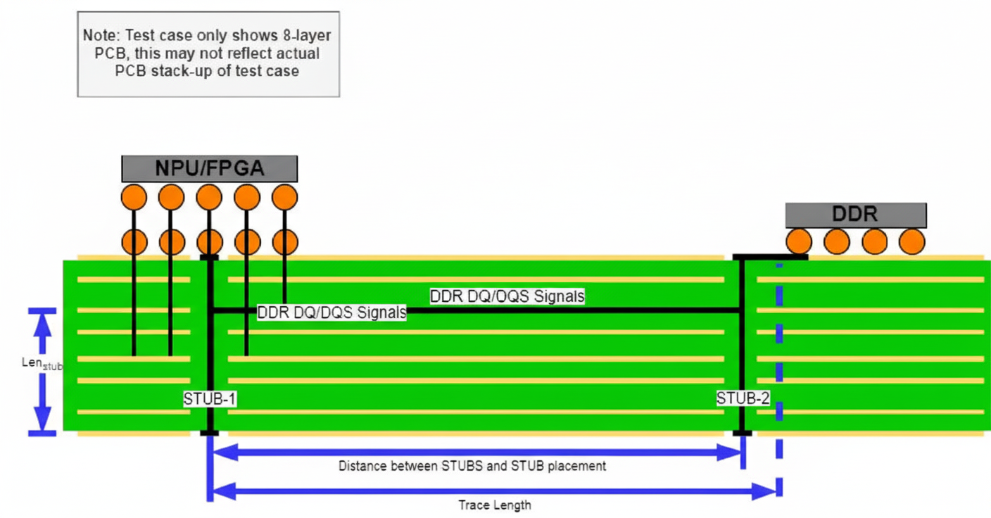
Test Case #2 models a static total channel length at 3200 Mbps, with only via discontinuities included in the channel. For all PCB stack-ups, the via structure is represented in the 3D depiction below. The via parameters were selected to achieve approximately a 10:1 aspect ratio with a 10 mil via diameter across stack-ups from 14 to 28 layers, targeting a median PCB thickness around 100 mils. Figures 2 and 3 show 2D depictions of the DDR4 data signal model with vias point-to-point and the channel model between the memory controller and the DDR4 memory, respectively.
The objective of Test Case #3 is to determine whether DDR4-3200 eye mask violations occur when the channel includes multiple discontinuities such as vias, a DIMM PCB, and a DIMM connector, compared to a channel of the same length in Test Case #2 without the DIMM interconnect. Figures 4 and 5 show the 2D model of a channel with a single DIMM per channel and the corresponding DQ channel model.
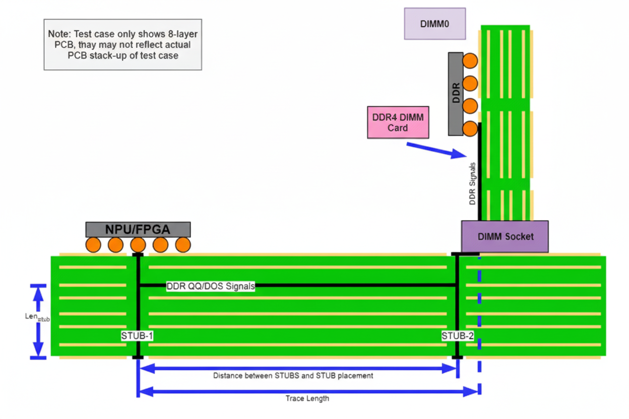
For Test Case #3, the ADS stack-up used an RDIMM fabrication table based on JEDEC RDIMM R/C-D1 format. The JEDEC RDIMM DQ net includes 15 ohm resistors in series with each DQ signal on the RDIMM, and that net structure was included in the test-case model.
Simulation and Results
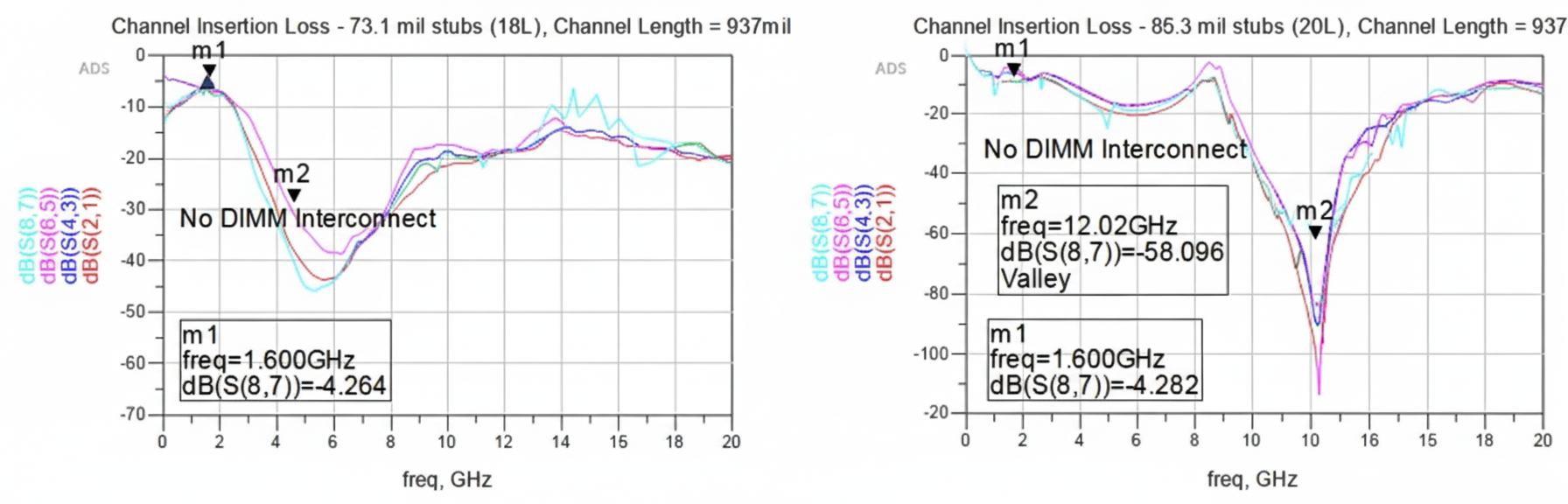
All eye mask simulations follow the JEDEC standard. For Test Case #2, the channel was tuned at 3200 Mbps for the best series resistor (Rs) and on-die termination (ODT) values. The results indicate that for a 937 mil channel with no equalization, the maximum stub length to meet DDR4-3200 eye mask compliance is 73.1 mils.
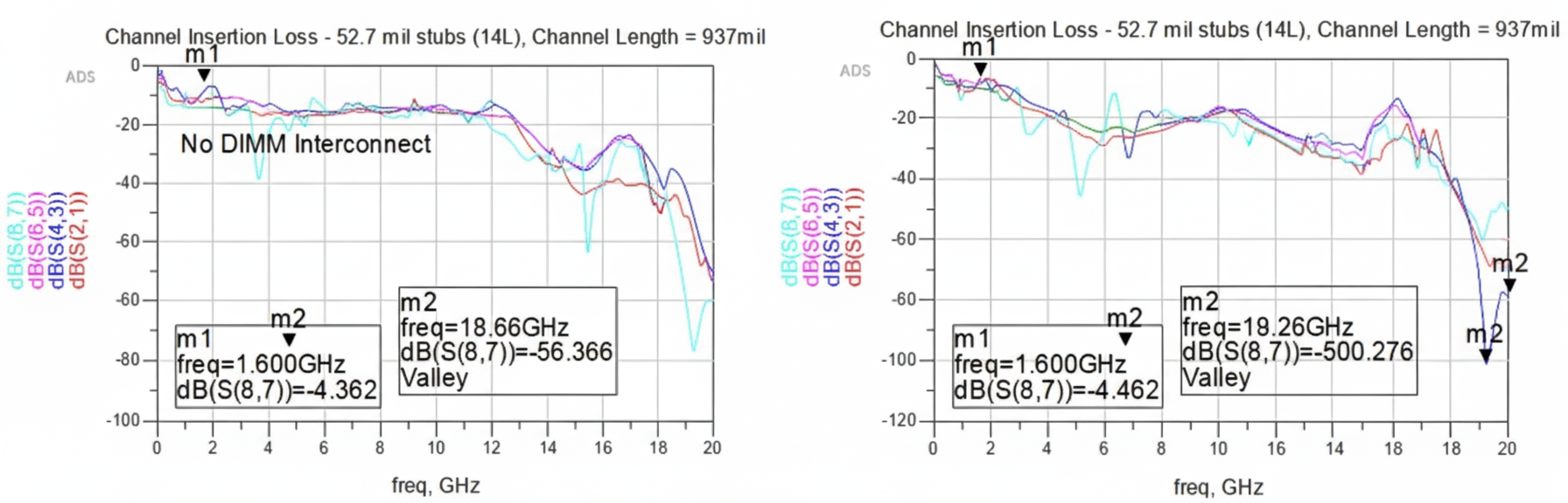
For Test Case #3, after tuning for Rs and ODT, the results show that even with a minimum available stub length of 52.7 mils, the DDR4-3200 compliance eye mask is not met. Further analysis routed data signals only on the top layer as microstrips to the DIMM interconnect, eliminating via stubs from the channel. Even with no via stubs, the DIMM interconnect alone still did not support DDR4-3200 due to discontinuity and loss introduced by the DIMM interconnect.
Channel Insertion Loss Analysis
Comparing channels with 73.1 mil and 83.3 mil stubs in Test Case #2 helps explain why one simulation passed and one failed. From 1.6 GHz to around 9 GHz the overall channel loss is similar, differing by a few dB. However, at 10 GHz (close to six times the DDR4-3200 clock frequency) the loss increases by 8 dB with an extra 10 mils of stub length, bringing total channel loss to roughly 20 dB. The channel with the 73.1 mil stub resonates near 14 GHz, while the 83.3 mil stub resonates near 12 GHz. There is about a 30 dB improvement in channel loss at 12 GHz with a 73.1 mil stub versus an 83.3 mil stub, which is a significant difference.
Comparing insertion loss for channels with 52.7 mil stubs in Test Case #2 and Test Case #3 shows that from 1.6 GHz to about 10 GHz the loss is similar, but at 14 GHz Test Case #3 suffers nearly 10 dB additional loss compared to Test Case #2. That extra 10 dB causes Test Case #3 to fail; total channel loss is close to 30 dB. The resonant frequencies are similar because stub lengths match, but the DIMM interconnect introduces the additional loss at resonance.
DDR4 Channel Eye Diagram Analysis
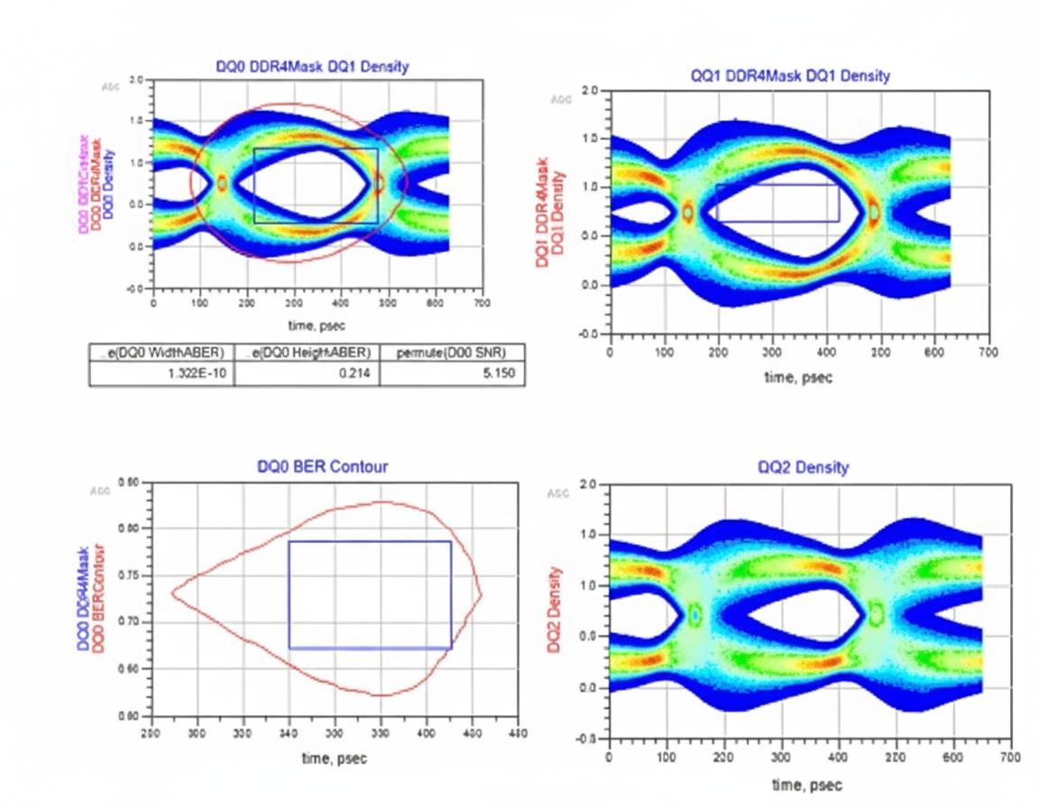
The simulation data was tabulated to produce the charts below. For Test Case #2, max eye diagram loss varies between about 2 percent and 30 percent depending on stub length, whereas for Test Case #3 the eye diagram loss approaches 100 percent.
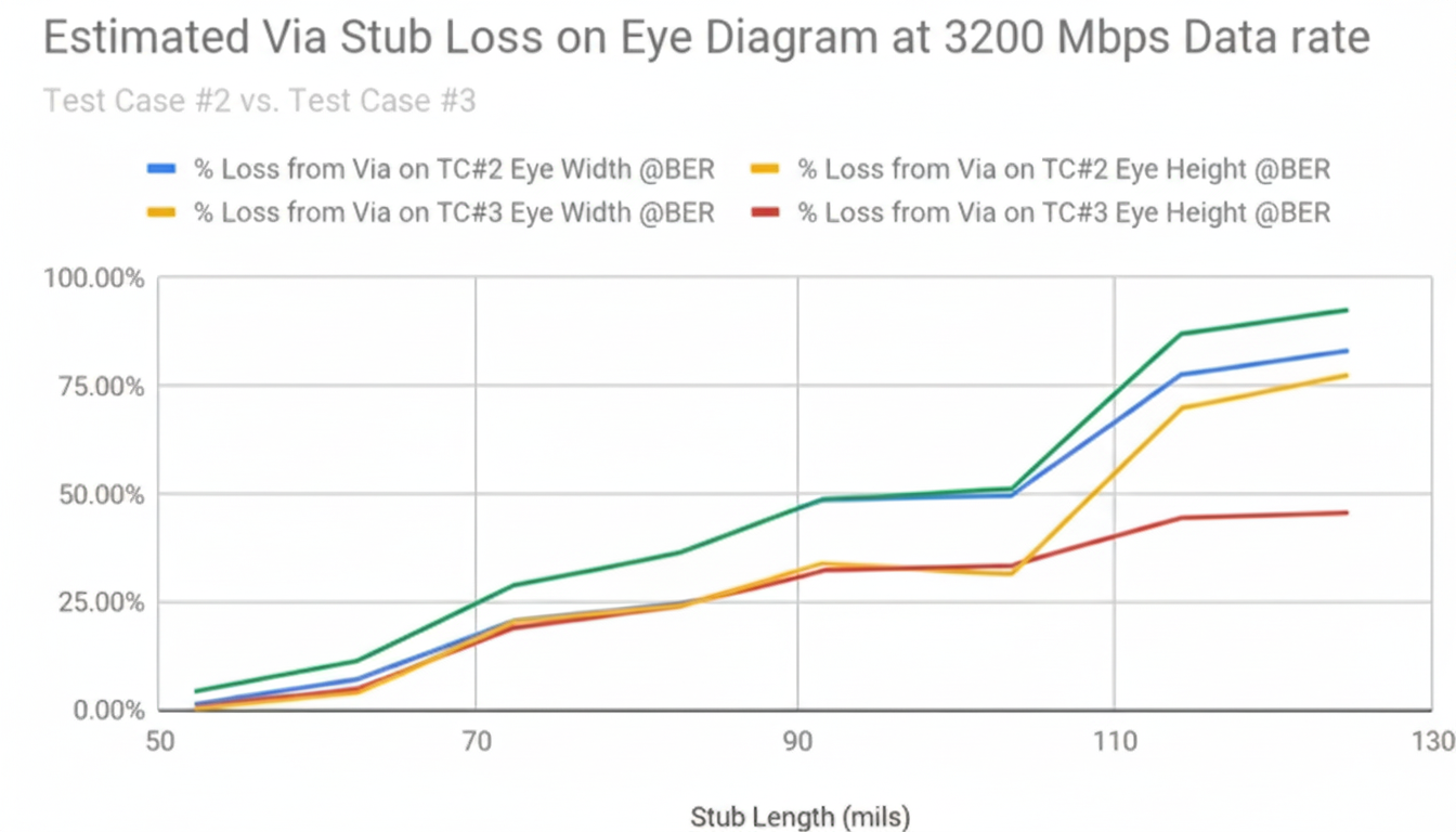
Figure analysis shows an 11.8 percent greater loss in eye height for Test Case #3 versus Test Case #2 with 73.1 mil stubs. Test Case #2 passed the DDR4-3200 eye mask at 73.1 mil stubs; this suggests the DIMM interconnect reduces eye height by about 12 percent. In Test Case #2 the 73.1 mil stub produced about 16 percent eye height loss, increasing to roughly 20 percent for an 83.3 mil stub. The eye mask violation for the 83 mil stub is attributable to signal reflections resonating near 12 GHz and overall channel loss approaching 30 dB.
JEDEC defines the DDR4-3200 DQ receive eye mask as 110 mV peak-to-peak with a timing window of 0.23 UI. In Test Case #3 the eye should have passed with 52 mil stubs but did not; the next section investigates why.
Deterministic Jitter Estimates
For Test Case #2 with 73.1 mil stubs, only 133 ps of margin is available, meaning 57.44% of the DDR4 data valid window is consumed by deterministic jitter. For DDR4-3200, 1 UI is 312.5 ps. With a 52.7 mil stub in Test Case #2, estimated deterministic jitter is about 156.2 ps, which consumes roughly 50% of the 1 UI valid window. Adding the DIMM interconnect consumes an additional 21% of the valid window through deterministic jitter, leaving almost no margin for valid data.
Conclusions
Design solutions for DDR4 channels must consider not only signal integrity but also power integrity and crosstalk from other signals, since those effects compound the problem. Simulation of the full channel with accurate models is essential. Analysis showed that without equalization, the maximum stub length for a DDR4-3200 point-to-point channel without DIMM interconnect is 73.1 mils. Vias introduce significant deterministic jitter to the channel.
Shrinking UIs introduce additional challenges. No solution was found in this study that passed the DDR4-3200 receive eye mask when both vias and a DDR4 DIMM interconnect were present. The DIMM interconnect alone adds enough loss to cause failures, and the problem becomes even more difficult for multi-DIMM-per-channel configurations. Simulation with equalization is required to mitigate DIMM interconnect losses and deterministic jitter.
Finally, the rule of thumb that interconnect bandwidth must be five times the Nyquist frequency is not sufficient for DDR4 channel design without considering full-channel effects and equalization. The entire channel must be designed in detail, with equalization playing a larger role for future DDR4 designs.