Overview
From HBM memory to 3D NAND chips and CoWoS, many devices in the hardware market are built using TSVs. TSV stands for Through-Silicon Via, a vertical electrical interconnect that passes through silicon to enable vertical communication between stacked dies. This article explains what TSVs are, how they work, and where they are used.
Origins and Early Development
In January 2000, Professor Sergey Savastiou at Santa Clara University published an article titled "Moore's Law - the Z dimension" in the journal Solid State Technology. The final chapter was titled "Through-Silicon Vias," which introduced the term Through-Silicon Via to the wider community. Around the same time, TSV-related technologies began to gain traction.
TSV Concept
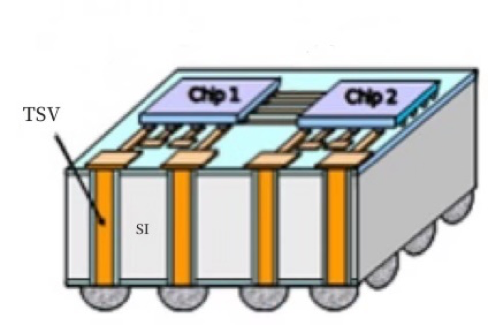
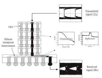
TSV is a vertical electrical interconnect that goes through a silicon substrate. While wire bonding and flip-chip bumping provide external electrical interconnects and redistribution layers (RDL) provide horizontal interconnects within a chip, TSV provides vertical interconnects through the silicon. As the only vertical interconnect technology, TSV is one of the core technologies in advanced semiconductor packaging.
Key Enabling Technologies
In the mid-1990s, the semiconductor industry transitioned to copper interconnects using the damascene copper plating process, replacing sputtered aluminum for transistor interconnects. The adoption of plated copper made metallization of TSV microvias by plating a practical approach. Two core technologies for modern TSVs therefore emerged: deep silicon etching and electroplating.
TSVs enable a third dimension of integration with the shortest electrical paths and improved noise immunity. As device scaling based on Moore's Law slows, miniaturization increasingly relies on TSV-enabled advanced packaging. TSVs are critical for devices such as CMOS image sensors (CIS), high-bandwidth memory (HBM), and silicon interposers. For CIS devices, signals often need to be routed from the back side, making TSVs essential. HBM is based on stacked memory dies; current implementations reach 12 layers and further increases rely on TSV interconnects. Silicon interposers enable integration of multiple chips such as CPUs, memory, and ASICs into a single package, and their vertical interconnects likewise depend on TSVs.
Consultancies such as Yole Development have found that TSVs can be applied to many chip packages and advanced packaging types, including LED and MEMS. Given TSVs' importance, foundry and OSTA companies have invested heavily in TSV research. A major development challenge has been ensuring that metal plating deposits primarily inside TSV holes rather than on the wafer surface. Without control, metal deposits on the wafer surface grow faster than inside TSV holes. Current solutions add suppressors and accelerators to the plating bath to inhibit deposition on the wafer surface while accelerating deposition inside the TSVs. Foundries and OSTA companies have optimized plating parameters such as current, temperature, wafer-to-electrode positioning, and additive concentrations, and equipment vendors have introduced tools targeted at TSV plating.
How TSVs Enable Vertical Communication
On most PCBs, most connections between chips are horizontal, meaning signals travel laterally on the board. CPUs in sockets connect vertically to the socket, but typical chips on boards are not vertically interconnected. TSVs enable vertical interconnection by passing vertical vias through different dies or layers in a stack, allowing direct vertical communication between them.
Applications and Advantages
One application of TSVs is partitioning a complex processor into several dies. Vertical connections allow a larger number of interconnects, increasing bandwidth without raising clock frequency, which would increase power consumption during data transfers. For example, future designs may place last-level caches off-die with the same bandwidth but several times the capacity, improving overall system performance. Intel's Foveros demonstrated a related approach for Lakefield SoC, where two parts of the SoC communicate through a die-to-die interconnect.
Partitioning a processor into smaller dies can improve yield: as die size grows, the probability of defects increases, reducing the yield of fully functional large dies. Using smaller dies can lower overall cost despite other trade-offs.
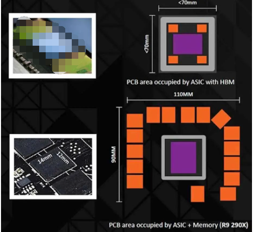
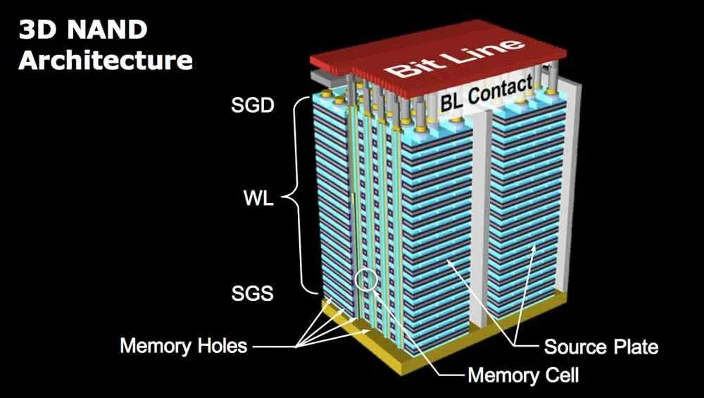
Another application relates to area efficiency. Vertically stacking multiple dies significantly reduces footprint compared with spreading dies across a board. A prominent example is using HBM for graphics memory. Another example is Samsung's V-NAND, which stacks multiple NAND flash layers. Less common options include stacking logic and memory where memory sits above the processor; examples include wide I/O memory used in some smartphones where memory on top of the SoC is connected via silicon interconnects.
On March 9, 2022, Apple introduced the M1 Ultra processor, which integrates multiple CPU complexes using a silicon interposer with TSVs. TSVs are increasingly important across AI/AR/VR sensors, image sensors, stacked memory, and high-performance processors.
Conclusion
TSV is a foundational packaging technology that enables vertical integration, higher bandwidth, reduced footprint, and improved signal integrity for stacked and heterogeneous systems. Its development and refinement continue to influence advanced semiconductor packaging and system design.