MEMS sensors and wireless sensor networks (WSNs) form the sensing backbone of modern electronics systems. In PCB manufacturing and design, integrating these components requires precise attention to layout, signal integrity, thermal management, EMI/EMC compliance, material selection, and high-reliability fabrication processes. Whether deployed in automotive safety systems, industrial IoT platforms, medical devices, or consumer wearables, sensor performance ultimately depends on optimized PCB implementation.
Common Sensor Types and PCB Integration Considerations
Sensors convert physical, chemical, or environmental parameters into electrical signals. Common categories include temperature, pressure, acceleration (accelerometers), angular rate (gyroscopes), magnetic field (magnetometers), humidity, gas, optical, and proximity sensors. Many are realized as MEMS devices fabricated on silicon wafers and then packaged for PCB mounting.
On the PCB, each sensor type imposes specific requirements:
- Accelerometers and gyroscopes demand low-noise analog or digital interfaces, minimal mechanical stress from board flexure, and careful placement away from vibration sources or heat-generating components.
- Temperature and humidity sensors require thermal isolation from power traces and proper ventilation or exposure to the environment while maintaining protection against moisture ingress.
- Magnetic sensors need shielding from nearby current-carrying traces and consistent orientation relative to the board's coordinate system.
PCB designers typically incorporate dedicated sensor footprints with appropriate land patterns, guard rings for noise immunity, and dedicated power planes or decoupling capacitors to ensure stable bias voltages.
MEMS Sensor Design Challenges on PCBs
MEMS sensors are sensitive to mechanical stress, temperature gradients, and electromagnetic interference. Effective PCB integration addresses these through:
- Symmetric layout and balanced copper distribution to minimize board warpage during reflow and thermal cycling.
- Use of high-Tg laminates and controlled stack-ups to reduce coefficient-of-thermal-expansion (CTE) mismatch with the sensor package.
- Optimized via placement and copper pours for heat dissipation without introducing parasitic capacitance or inductance.
- Signal conditioning circuits (amplifiers, ADCs, filters) placed close to the sensor to shorten analog traces and preserve signal integrity.
High-density interconnect (HDI) technology and micro-vias enable compact multi-sensor modules while maintaining routing density. In automotive and aerospace applications, additional requirements include AEC-Q100 qualification, vibration resistance, and long-term drift compensation through calibration algorithms stored in onboard memory.
Wireless Sensor Networks and PCB Requirements
Wireless sensor networks combine sensing, processing, and radio communication in distributed nodes. PCB design for WSN nodes must balance power consumption, RF performance, and reliability:
- Antenna design and placement are critical—PCB trace antennas, chip antennas, or external connectors require impedance-controlled routing (typically 50 Ω) and clearance from ground planes.
- Power management circuitry (DC-DC converters, energy harvesting interfaces) needs low-EMI layouts and efficient thermal paths.
- Microcontroller and radio SoCs demand careful partitioning of digital, analog, and RF sections with proper grounding schemes (star or hybrid) to prevent noise coupling.
- Battery or energy-harvesting integration influences board thickness, connector choice, and conformal coating for environmental protection.
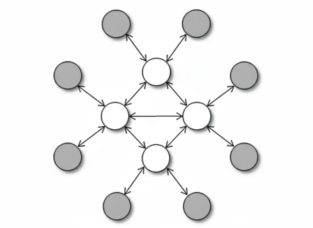
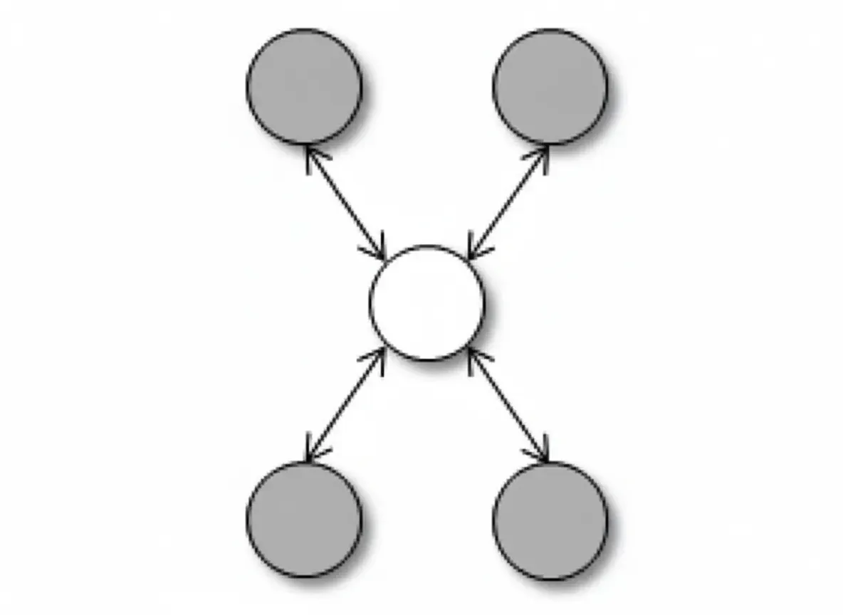
Mesh or star topologies common in industrial IoT further require robust firmware support and PCB-level provisions for over-the-air updates and diagnostics.
Nanosensors and Emerging PCB Technologies
Nanosensors leverage nanomaterials such as carbon nanotubes, graphene, or quantum dots to achieve ultra-high sensitivity and miniaturization. Their integration on PCBs introduces new challenges and opportunities:
- Ultra-fine pitch interconnects and advanced surface finishes (ENIG, OSP, or immersion silver) ensure reliable electrical contact with nanoscale elements.
- Flexible or rigid-flex PCBs accommodate wearable or conformal sensor arrays where traditional rigid boards are unsuitable.
- Embedded sensor elements within the PCB stack-up (e.g., printed or deposited sensing layers) reduce assembly steps and improve reliability.
- Specialized materials with enhanced thermal conductivity or low dielectric loss support high-frequency nanosensor readouts.
These technologies are increasingly adopted in environmental monitoring, biomedical diagnostics, and structural health monitoring, where PCB manufacturers must support cleanroom-compatible processes and tight tolerance control.
Sensor Roadmap, AI Integration, and Future PCB Optimization
Over the next decade, sensors will become more intelligent, energy-autonomous, and densely integrated. Key trends include:
- Edge AI and machine learning directly on sensor nodes, requiring PCBs with high-performance processors, high-bandwidth memory interfaces, and advanced thermal solutions.
- Multi-modal sensor fusion on single boards or modules, driving demand for HDI, embedded components, and heterogeneous integration.
- Energy harvesting and ultra-low-power design pushing PCB layouts toward minimal leakage and optimized power planes.
- 5G/6G connectivity and massive IoT deployments necessitating millimeter-wave compatible materials and precise RF layout techniques.
Robotics and big-data ecosystems further amplify the need for synchronized, high-accuracy sensor arrays with deterministic timing and robust communication protocols—all of which are enabled by sophisticated PCB design.

Conclusion
MEMS sensors, nanosensors, and wireless sensor networks deliver transformative capabilities only when seamlessly integrated at the PCB level. By addressing mechanical stress, signal integrity, thermal management, RF performance, and advanced manufacturing processes from the earliest design stages, engineers achieve higher accuracy, lower power consumption, and greater long-term reliability. As sensor density and intelligence continue to rise across automotive, industrial, medical, and consumer applications, specialized PCB solutions remain the critical foundation for scalable, high-performance sensing systems. Aivon's advanced manufacturing capabilities—including HDI, heavy copper, flexible substrates, and precision RF features—enable the next generation of intelligent sensor platforms.