Introduction
Resistive touch panels, due to their multilayer material stack, have lower optical transmission and reduced accuracy in locating finger position compared with capacitive touch panels. When capacitive touch uses charge-transfer techniques in a transverse-mode configuration, it can address noise and signal-to-noise issues and produce a more robust capacitive touch solution.
Because touchscreens are responsive and intuitive to use, they have been widely adopted in consumer electronics, industrial devices, and commercial systems such as ticketing terminals as user interfaces.
Earlier Touch Technologies
Touchscreen concepts were proven decades ago, but early technologies were not suitable for low-cost mass-market applications. These included infrared systems and surface acoustic wave sensing. Infrared systems used arrays of sensors in horizontal and vertical directions to detect a finger interrupting modulated light beams. Surface acoustic wave sensors detected absorption of acoustic waves by a finger near the screen surface, allowing detection of a touch based on changes to the acoustic signal.
Besides those methods, other options exist, but the mainstream trends today are resistive and capacitive sensing. Both approaches have advantages, but capacitive controller ICs simplify single-touch applications and can enable multi-touch capabilities that resistive systems cannot provide.
Limitations of Resistive Touch Panels
Resistive touch panels have been refined since the 1970s. The basic structure consists of two conductive transparent layers separated by small spacers that create a thin air gap. Typically, indium tin oxide (ITO) is deposited on a plastic film and a glass substrate. The top layer is flexible and the bottom layer is rigid, with many tiny transparent spacer dots between them. When a user presses the top layer, a contact forms and a voltage gradient is created; the controller senses this and computes X and Y coordinates.
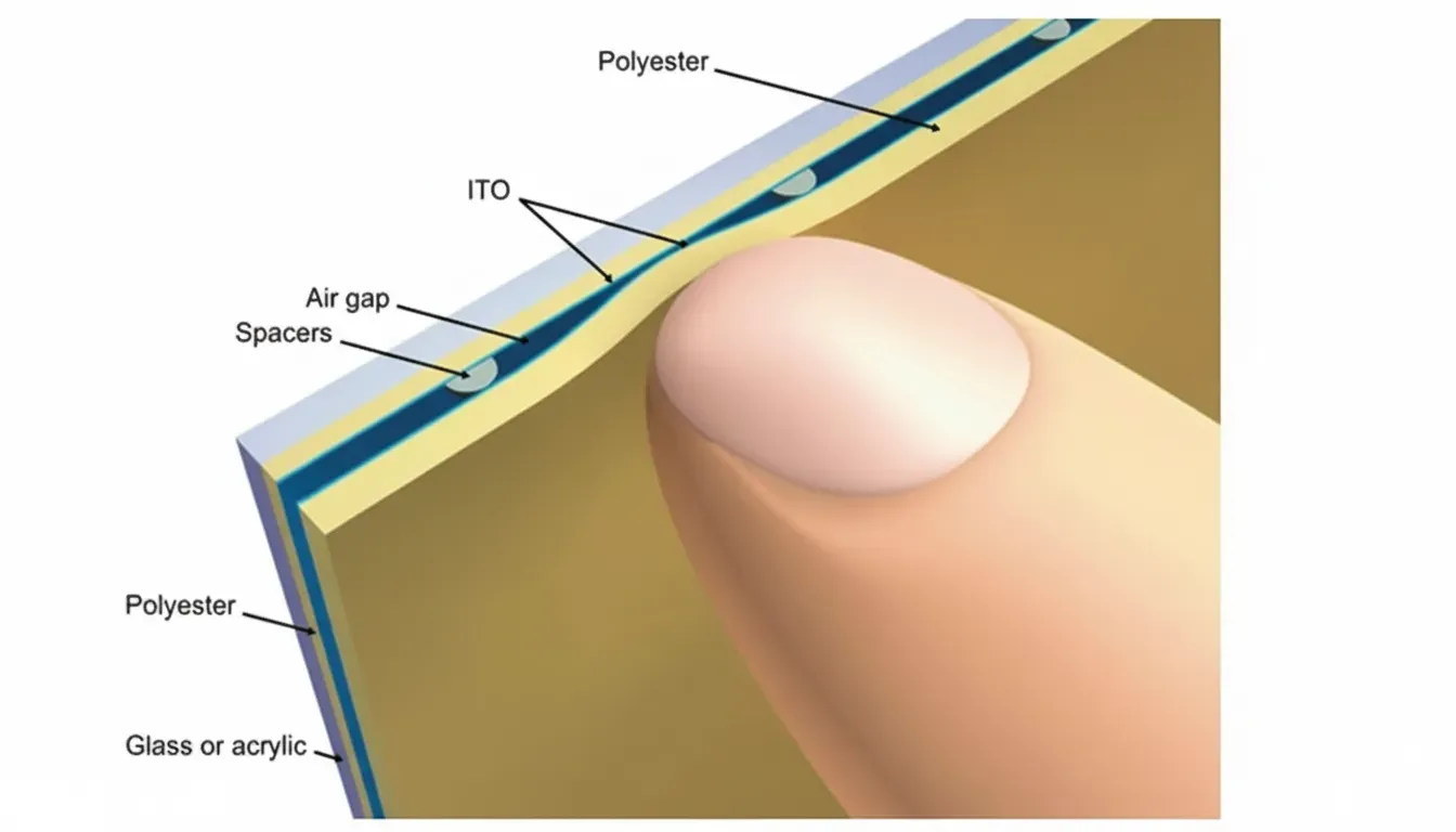
Figure 1: Resistive touch panel schematic
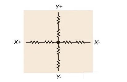
Figure 2: Four-wire resistive touch electrode potentiometers
In a simple four-wire resistive configuration, each of the two layers has two electrodes at opposite ends. The electrodes are orthogonal between layers, forming a four-wire star configuration equivalent to a pair of orthogonal potentiometers. To measure the X position, the controller biases X- to ground and X+ to a reference voltage, then reads voltage from the Y layer endpoints to find the X contact position. To determine Y, the controller drives the Y layer electrodes and reads the voltage on the X layer.
Variants include five-wire systems, where the substrate has an ITO coating and electrodes on all four edges plus a flexible membrane as the fifth electrode. When pressed, the controller measures voltages on X and Y to determine touch. Other variants, designed for larger displays and higher resolution, use six-wire or eight-wire systems.
Resistive technology's main advantage is a simple interface: the controller applies a reference voltage to one pair of electrodes and reads the potential on the other pair. On-chip MOSFET switches, analog multiplexers, and ADCs can implement this easily. With differential ADC measurements, the result becomes radiometric and can use Vcc and ground as stimuli, enabling very high resolution with proper design.
However, resistive panels suffer from their multilayer stack. The substrate is typically glass with uniform ITO, the top layer is usually PET with ITO on its inner surface and a hard coating on the outer surface for protection, and transparent spacer dots are produced during printing. The stacked structure reduces optical transmission, typically to around 75% of clear glass. The air gap can introduce haze and reduce clarity. The structure is also vulnerable to scratches, requires careful mechanical alignment to establish X and Y coordinate ranges, and is susceptible to electrical noise, especially from the LCD. Filtering to remove that noise can increase response time. Also, resistive controllers typically handle only a single touch point, which is a significant limitation.
Charge-Transfer Techniques for Capacitive Sensing
Because of resistive limitations, many designers have shifted to projected capacitive sensing. Capacitive controller ICs implement several circuit approaches: RC time-constant measurement circuits (oscillators), AC current measurement blocks, and charge-transfer blocks. Charge-transfer circuits can operate in single-ended or transverse-mode; any approach can be applied to electrode arrays on two or more layers to create a touchscreen.
RC time-constant techniques measure changes in charge/discharge time when a capacitance C changes due to a finger. They can measure frequency or time, in free-run or single-cycle modes. RC methods tend to be slower, sensitive to leakage currents, limited in dynamic range, hard to calibrate, and subject to drift. Their high impedance makes them vulnerable to external noise, so their use has declined.
AC current measurement drives the impedance with an AC source and measures voltage across the impedance to infer Cx. These circuits share many RC limitations, although they typically use lower drive impedance. They require amplifiers to recover small voltages, which introduces signal-to-noise concerns. AC methods are used in some panels, particularly those with low-impedance front surfaces.
Single-ended charge-transfer capacitive sensors use one electrode per sensing channel. They do not rely on timing or amplifiers but use CMOS switches to pump charge into Cx and transfer charge to a reference sampling capacitor Cs. The circuit counts the number of cycles required for Cs to reach a preset voltage; this cycle count is inversely proportional to Cx. Charge-transfer techniques suppress leakage current effects and, because a relatively large Cs is used as the detector, the detector presents a low impedance to external electrical noise, improving immunity.
Transverse-Mode Charge-Transfer Sensing
Transverse-mode charge-transfer sensing uses two electrodes per sensing element. Electrically, it behaves similarly to single-ended charge-transfer sensing but implements a transmit/receive matrix of electrodes to realize a touchscreen. Advantages include reduced routing, the ability to distinguish multiple simultaneous touch points, faster speed, and lower power consumption. Because all nodes on a drive line can be measured simultaneously, acquisition cycles can be reduced by about 50% compared with sequential single-ended scans.
The dual-electrode structure provides self-shielding against external noise and improves signal stability at a given power level. Some suppliers have implemented transverse-mode sensing combined with high-load sampling modes, spread-spectrum modulation, and digital signal processing to increase robustness against noise sources, producing solutions that remain stable even in challenging environments.
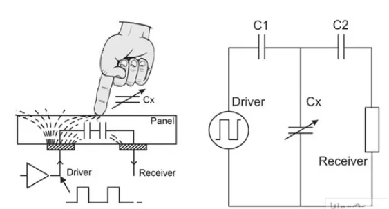
Electrically, transverse-mode sensing resembles a T-bridge attenuation network, where the user finger acts as a coupling capacitance Cx between a pair of electrodes. A finger touching the screen surface absorbs coupled charge between drive and receive electrodes, and much of the charge returns to ground via stray capacitance paths, reducing the measured signal amplitude. The reduction is measurable and proportional to the coupling.
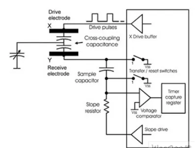
Figure 3: Transverse-mode sensing principle
Despite very low power consumption, transverse-mode sensors can detect multiple fingers through several millimeters of plastic, glass, or other materials. Electrodes can be made from any conductive material such as ITO and can take many sizes and shapes. Noise reduction algorithms help suppress noise from modules like LCDs, often without a separate shielding layer. This improves display light transmission and can reduce construction cost and backlight power requirements. Some transverse-mode controller implementations use a dual-slope conversion form to ensure high temporal and thermal stability.
Pulse-Train Sampling and Zero-Cross Timing
Controller ICs collect signals coupled into receive electrodes on a sampling capacitor synchronized with drive pulses and use pulse trains to improve signal-to-noise ratio. The number of pulses in each train directly affects circuit gain and can be adjusted to match different panel materials, key sizes, and panel thicknesses.
The pulse train creates a stepped ramp waveform on the sampling capacitor. After the pulse train, the driver switches the reference of the ramp resistor to a high level to discharge the sampling capacitor until the charge is exhausted. A voltage comparator detects the zero-cross point. The ramp time required to reach the zero-cross point is proportional to the X and Y charge coupling and decreases when a finger touches the panel surface.
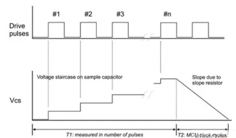
Figure 5: Ramp time proportional to X and Y charge coupling
This automatic zeroing behavior makes the circuit resilient to variations in supply voltage and parameters such as Cs. The technique also provides inherent moisture suppression and RF immunity. For example, small local water films on the panel surface slightly increase coupling, while a user’s finger decreases coupling. Moisture can cause erroneous polarity changes and false touches in other solutions. Because a surface water film can be modeled as a time-dependent distributed RC network, using very short gate times for charge collection (microseconds or shorter) suppresses the water film effect.
Single-Layer Touch Panels
Because controller ICs can perform most signal conditioning on-chip, only a few discrete resistors and capacitors are required, plus a simple serial interface such as I2C. From a firmware perspective, the IC exposes a simple command set and register map, so designers mainly need to design the sensing matrix and implement the interface code. Projected capacitive touch requires an X,Y transparent electrode matrix to determine finger position.
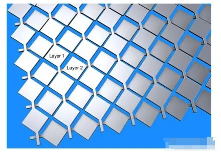
Figure 6: X,Y transparent electrode matrix for projected capacitive screens
Traditionally two or more ITO-coated layers are laminated on glass or plastic lenses, and each added layer increases cost and reduces light transmission by approximately 9%. Therefore, minimizing layer count is desirable. Although touch-controller ICs support multilayer diamond patterns, they can also work with proprietary single-layer film techniques. Compared with multilayer approaches, single-layer film electrodes offer higher transparency, thinner profiles, and lower cost, which makes them attractive for many designs.
Dual-Axis Multi-Touch
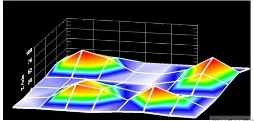
Single-layer films can perform dual-touch detection synchronously, but dual-layer designs that resolve multi-touch events simultaneously offer superior performance. In a lab model, 3D electric field measurements show distinct signatures for three fingers plus a thumb.
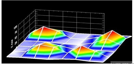
Figure 7: 3D electric field measurement with multiple fingers
By connecting an eight-electrode X layer to a six-electrode Y layer, a controller can support up to an 8-inch dual-touch panel. Such controllers can sense up to six sliders or 48 discrete keys, or combinations of keys, sliders, and touch regions. A compact-pin-count version can drive eight X lines and receive four Y lines, distinguishing up to 32 discrete keys with similar simple wiring.
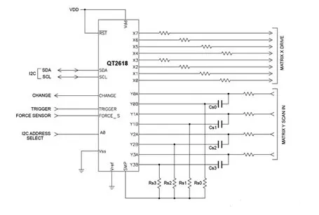
Figure 8: Controller circuit diagram
Ramp resistor values that directly affect gain are typically on the order of megaohms; optional series resistors in X and Y directions can improve EMC performance and ESD robustness, typically in the 1–20 kΩ range. In addition to controllers, vendors provide touchscreen demonstration and test toolkits so designers can validate gestures and interaction behaviors such as two-finger spreads, local zoom, map panning, rotation gestures for 3D objects, and game controls. Simple design tools in these kits can inspire novel user interfaces and accelerate product differentiation.