Overview
To enable efficient information transfer and communication, 5G and future 6G networks require more antennas, larger bandwidth, and higher base station density. Demand for radio-frequency (RF) electronic components is expected to rise substantially. For example, by 2025 the global number of 5G base stations was projected to reach tens of millions. The rapid growth of RF electronic devices, particularly mobile terminals, also raises concerns about electromagnetic pollution and environmental impacts from electronic waste.
For decades, conductive materials used in RF devices and electromagnetic interference (EMI) shielding have been metal-based. However, increasing requirements for flexibility, high integration, light weight, manufacturability, and operation at higher frequencies make traditional metal structures less suitable. At the same time, the environmental impact of growing volumes of electronics makes sustainability for next-generation consumer devices increasingly important.
Researchers led by Prof. He Daping at Wuhan University of Technology proposed a graphene assembled film (GAF) that can replace copper in practical electronic products such as RF components and EMI shielding.
Advantages of GAF
Corrosion resistance of GAF antennas
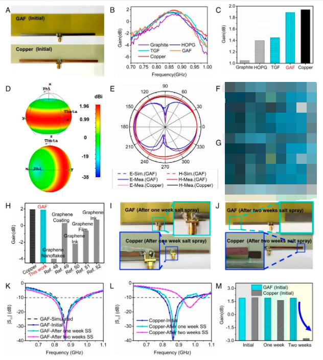
Figure 1: GAF used as a dipole antenna and its corrosion performance. (A) Digital photos of GAF and copper dipole antennas. (B) Measured gain across bandwidth for antennas made from different materials. (C) Gain of different-material antennas at 865 MHz. (D) Simulated 3D radiation pattern of the GAF antenna. (E) E-plane and H-plane radiation patterns of GAF and copper antennas. (F and G) Measurement setups for E-plane and H-plane radiation patterns. (H) Comparison of dipole antenna gain from reference works with results in this work. (J) Digital photos of GAF and copper dipole antennas after 1 week and 2 weeks of salt fog exposure. (K) Measured and simulated |S11| of the GAF antenna: initial, after 1 week, and after 2 weeks of salt fog. (L) Measured |S11| of the copper antenna: initial, after 1 week, and after 2 weeks of salt fog. (M) Measured gain at 865 MHz for GAF and copper antennas under initial, 1-week, and 2-week salt fog conditions.
After two weeks of salt fog exposure, the GAF antenna maintained gain, reflection coefficient, and other electrical properties, while the copper antenna was corroded and degraded.
Wider operational bandwidth
GAF ultra-wideband antennas cover from 3.7 GHz to 67 GHz, providing a bandwidth of 63.3 GHz, which is about 110% greater than comparable copper-foil antennas. Compared with copper antennas, GAF-based 5G antenna arrays show wider bandwidth and lower sidelobe levels. The researchers also demonstrated that GAF metasurfaces, serving as flexible frequency-selective surfaces (FSS), exhibit promising frequency-selective characteristics and angle stability.
High conductivity
GAF electrical conductivity reaches approximately 2.58e6 S/m. After 200,000 bending cycles with a bending radius of 1.5 mm, the graphene assembled film retained high flexibility and conductivity without structural damage. To evaluate applicability in 5G and flexible electronics, the team demonstrated flexible coplanar waveguide (CPW) transmission lines and resonators based on graphene and measured stable performance under various bending and twisting conditions. Graphene-based dipole antennas exhibit good reflection coefficients and high gain, comparable to copper antennas.
Superior EMI shielding
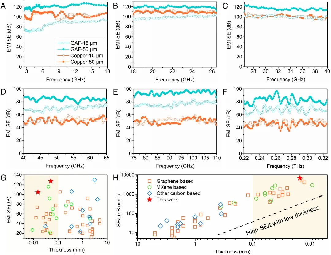
Figure 2: GAF applied to EMI protection. (A–F) EMI shielding effectiveness (SE) for 15 μm and 50 μm GAF and for 10 μm and 50 μm copper over the frequency ranges 2.6 GHz to 0.32 THz: (A) 2.6–18 GHz (rectangular waveguide method), (B) 18–26.5 GHz (rectangular waveguide), (C) 26.5–40 GHz (rectangular waveguide), (D) 40–67 GHz (free-space method), (E) 75–110 GHz (free-space), and (F) 0.22–0.3235 THz (free-space method).
GAF EMI shielding effectiveness (SE) outperformed copper, reaching up to 127 dB over 2.6 GHz to 0.32 THz. On a per-thickness basis, SE reached 6,966 dB/mm, better than copper of comparable thickness.
Beyond full shielding, selective shielding of electromagnetic bands is often important to preserve transmission in other bands. As a member of metamaterials, frequency-selective surfaces (FSS) are formed by periodic structural units and can selectively absorb, reflect, or transmit electromagnetic waves, enabling frequency selection. The GAF FSS maintained frequency-selective performance when bent from 0 to 40 degrees and retained good selection performance for incident angles within plus/minus 30 degrees, demonstrating high angular stability.
GAF Fabrication
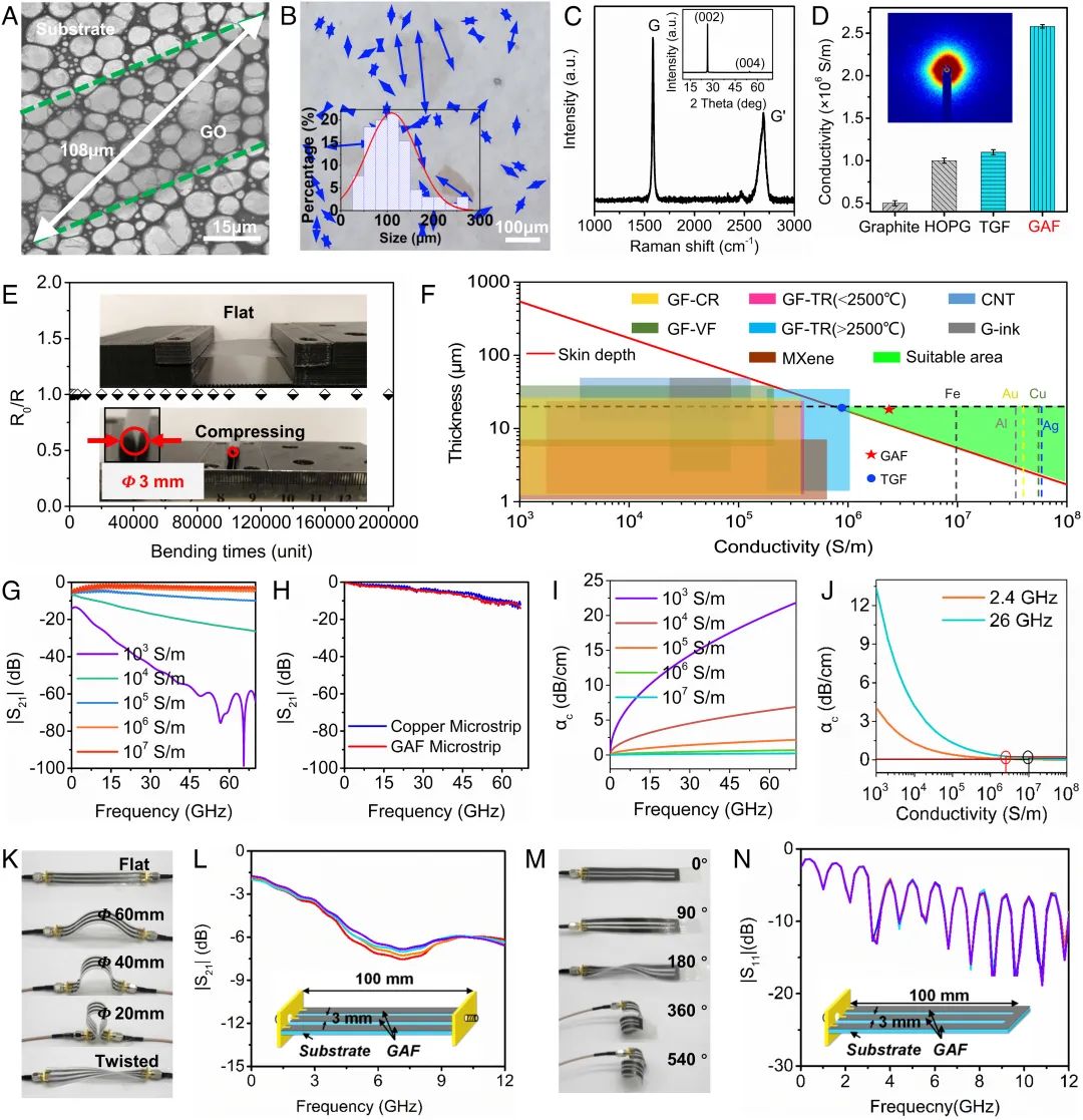
Figure 3: GAF characterization. (A) TEM image of a typical large graphene oxide (GO) flake with lateral dimension of about 108 μm. (B) Optical microscope image of large GO (LGO) sheets prepared by drop-casting on SiO2; inset shows statistical lateral-size distribution. (C) XRD pattern and Raman spectrum of GAF. (D) Summary of electrical conductivity for GAF, graphite, highly oriented pyrolytic graphite (HOPG), and typical flake-size GO assembled films (TGF); inset shows SAXS pattern. (E) Resistance change of GAF after 200,000 repeated bending tests, demonstrating long-term flexibility and stability. (F) Skin depth at 860 MHz as a function of conductive layer thickness for materials prepared by chemical reduction, vacuum filtration, thermal reduction of GO films, graphene flakes, graphene ink, carbon nanotubes (CNT), and MXene. (G and H) Simulated (G) and measured (H) transmission coefficients of the microstrip transmission line (MTL). (I and J) Conductor loss for different frequencies (I) and conductivities (J). (K) Flexible GAF FCPW transmission line bent to diameters of 60 mm, 40 mm, 20 mm and twisted by 180 degrees. (L) Transmission coefficient of the FCPW from 10 MHz to 40 GHz under different mechanical states. (M) Flexible GAF quarter-wave shorted resonators under twist conditions: untwisted, 90, 180, 360, and 540 degrees. (N) Reflection coefficient results of the resonators between 10 MHz and 12 GHz under different twist conditions.
Two main approaches were used to achieve high conductivity in graphene laminate plates. First, the team maximized graphene microcrystal size, reducing the impact of contact resistance. Second, a secondary annealing process and a specialized assembly technique enabled highly laminated, defect-minimized continuous films from large graphene microcrystals.
Graphene oxide (GO) was prepared by an improved Hummers method. Large GO (LGO) flakes were separated and collected as the precursor for film fabrication. After seven repeated centrifugation steps, LGO was isolated from a 3 wt.% GO suspension (collecting the bottom 30% of GO each time). Optical microscopy-based lateral-size statistics show that 74% of LGO flakes exceed 75 μm, and 54% exceed 100 μm. Typical flake-size GO (TGO) was used as a control sample. LGO assembled films were fabricated by roll transfer coating of premeasured LGO hydrogel onto a self-peeling substrate such as PET film.
The LGO hydrogel on the substrate was dried at 70–80 °C. After drying, a soft, deep-brown freestanding paper-like GO film (LGO film) could be peeled from the PET substrate. During this step, the anisotropic liquid-crystalline behavior of the LGO hydrogel can produce prealigned oriented structures after force-directed roll transfer.
This highly ordered laminate was converted to graphitized material via high-temperature graphitization. LGO films were thermally annealed between two graphite plates in an argon atmosphere at 1,300 °C for 2 hours and at 2,850 °C for 1 hour for reduction and graphite crystallization. Large crystalline graphite domains in GAF result from merging of neighboring reduced LGO flakes.
After initial high-temperature annealing, the material becomes fully graphitized, allowing defect-free graphene nanosheets to lie flat and make large-area planar contacts. Subsequent rolling compression under 300 MPa pressure yields the final GAF. Rolling compression helps eliminate interlayer gaps and contact resistance and contributes to excellent flexibility.
Following rolling, a second high-temperature anneal at 2,850 °C in argon removes structural damage introduced during rolling and further improves conductivity. Using the same procedure but starting from TGO produces TGF.
Conclusion
The research team demonstrated progress in lightweight, flexible, mechanically durable, chemically stable, and highly conductive GAF structures that can be applied to multi-band 5G wireless communication equipment and electromagnetic protection, addressing key limitations of copper-based electronics. GAF-based 5G electronic components can be designed in complex patterns and integrated into communication systems to support advanced functions across microwave communication bands.
GAF also shows excellent electromagnetic shielding performance in microwave and terahertz bands and can be fabricated into metamaterials for selective electromagnetic shielding. The study indicates that highly conductive graphene films can serve as a full-function, sustainable alternative material for RF applications, supporting current and next-generation flexible electronics, wireless communication equipment, and EMI shielding. Macroscopic graphene films can act as functional and more sustainable replacements in current and future devices.