5G networks demand denser base stations, wider bandwidths, and higher antenna counts to support multi-gigabit data rates across microwave and millimeter-wave bands. These requirements increase the need for radio-frequency (RF) components that maintain performance while meeting stricter constraints on weight, flexibility, integration density, and long-term reliability. Traditional copper-based conductors and shields face limitations in high-frequency operation, mechanical flexibility, and environmental durability, particularly in corrosive or high-vibration environments.
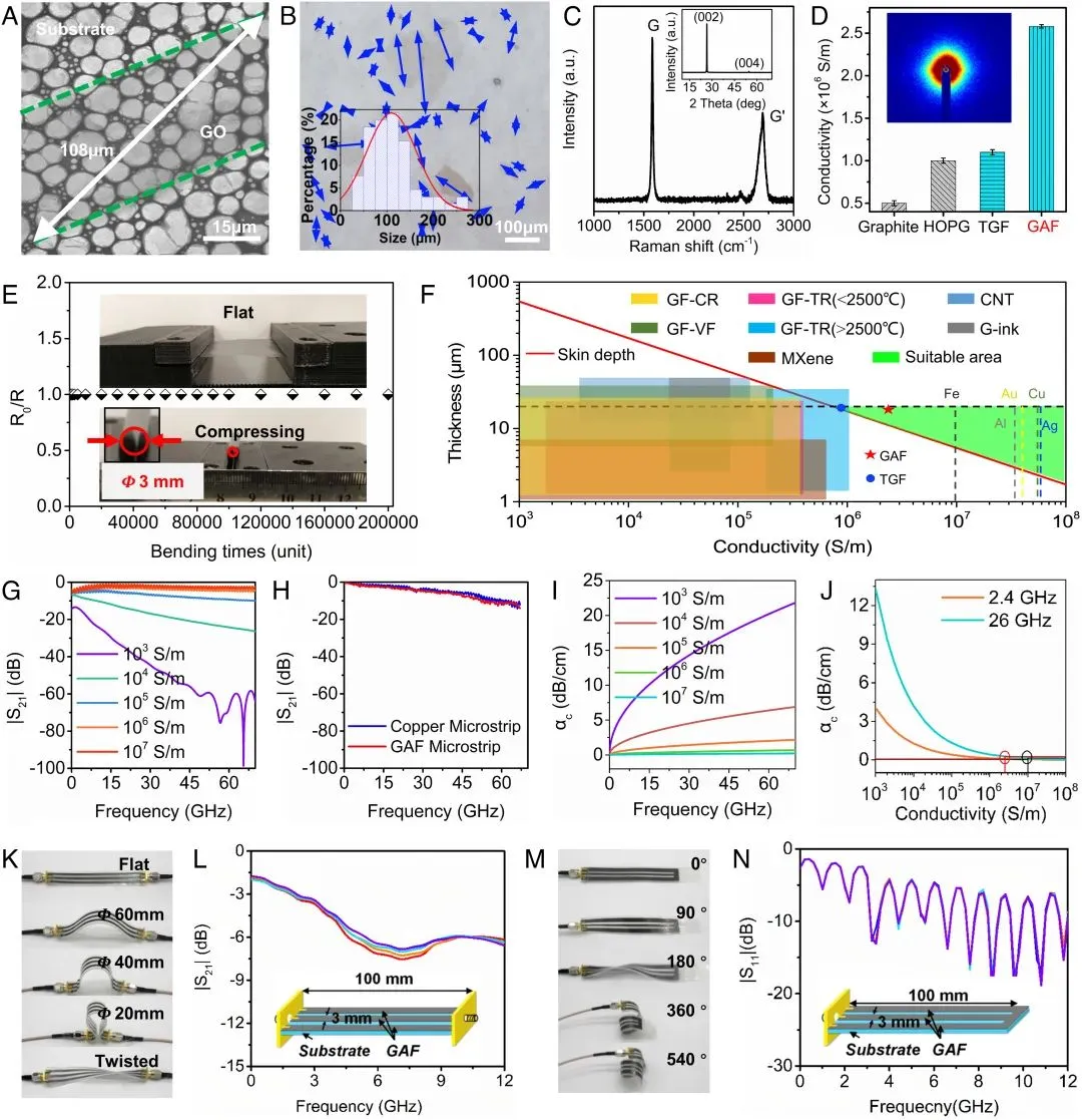
Graphene assembled film (GAF) has emerged as a candidate material that addresses several of these constraints. Developed through controlled assembly of large graphene oxide flakes followed by high-temperature graphitization and compression, GAF achieves electrical conductivity of approximately 2.58 × 10⁶ S/m while retaining mechanical flexibility after repeated bending.
Electrical and RF Performance Characteristics
GAF exhibits skin-depth behavior comparable to metals at 5G-relevant frequencies while delivering measurable advantages in bandwidth and stability. Ultra-wideband dipole antennas fabricated from GAF cover 3.7–67 GHz (63.3 GHz bandwidth), representing roughly 110 % greater fractional bandwidth than equivalent copper-foil designs. In antenna arrays, GAF versions demonstrate wider operational bandwidth and reduced sidelobe levels. Coplanar waveguide transmission lines and quarter-wave resonators built on GAF maintain stable S-parameters under bending radii down to 1.5 mm and twist angles up to 540°, confirming suitability for flexible RF interconnects.
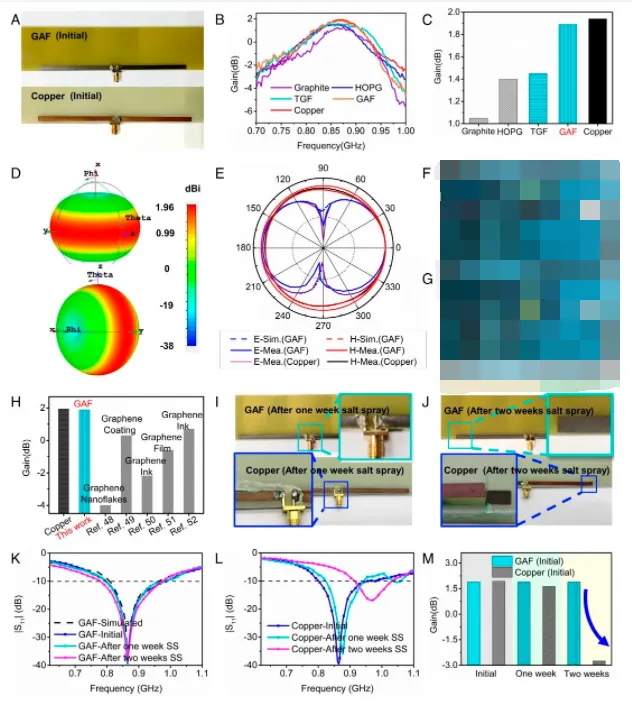
Electromagnetic interference (EMI) shielding effectiveness reaches 127 dB across 2.6 GHz to 0.32 THz. On a normalized per-thickness basis, shielding performance exceeds 6,966 dB/mm—higher than copper foils of similar thickness. Frequency-selective surfaces (FSS) patterned from GAF retain angular stability up to ±30° incidence and maintain selectivity when bent to 40°, enabling selective band filtering without compromising adjacent transmission windows.
Corrosion Resistance and Mechanical Durability
Salt-fog exposure testing reveals a decisive reliability advantage. After two weeks, GAF dipole antennas retain original gain, reflection coefficient, and radiation patterns, whereas copper antennas exhibit visible corrosion and measurable degradation in |S11| and gain. This stability stems from the absence of electrochemical oxidation pathways present in metals. After 200,000 bending cycles at 1.5 mm radius, GAF conductivity and structural integrity remain unchanged, supporting applications in foldable or wearable 5G devices.
Fabrication Process and Material Engineering
GAF production begins with an improved Hummers-method graphene oxide suspension enriched in large flakes (≥75 µm lateral size for 74 % of particles). Repeated centrifugation isolates these large flakes, which are then roll-transfer-coated onto a sacrificial substrate to form oriented liquid-crystalline films. Thermal annealing at 1,300 °C followed by 2,850 °C under argon merges flakes into large crystalline domains. Final rolling at 300 MPa eliminates interlayer voids, after which a second 2,850 °C anneal restores any lattice damage and maximizes in-plane conductivity. The resulting film is freestanding, paper-like, and compatible with conventional patterning techniques such as laser cutting or photolithography.
Integration Considerations for PCB and Flexible Circuit Manufacturing
High-frequency PCB and flexible printed circuit (FPC) designs require conductor materials that support controlled impedance, low insertion loss, and compatibility with multilayer lamination and soldering processes. GAF's planar laminate structure and thermal stability up to graphitization temperatures align with existing PCB fabrication workflows, including roll-to-roll processing and laser direct imaging. Its flexibility enables direct integration into bendable RF modules without additional strain-relief features required for brittle copper traces. Thermal management benefits arise from graphene's in-plane conductivity, potentially reducing hotspot formation in densely packed 5G power amplifiers or phased-array modules.
Reliability engineering must still address interface adhesion between GAF and dielectric substrates, via formation for multilayer boards, and long-term electromigration under high current densities. Environmental testing protocols already used for copper (temperature-humidity-bias, thermal cycling, and mixed flowing gas) apply directly, with early data indicating superior corrosion performance.
Industry Trends and Design Implications
The shift toward millimeter-wave 5G and early 6G research emphasizes materials that combine high conductivity with mechanical compliance and sustainability. GAF addresses electromagnetic pollution concerns by enabling thinner, more effective shields and supports circular-economy goals through reduced metal content and improved recyclability potential. For system designers, the ability to pattern complex metasurfaces and FSS directly on flexible substrates opens new architectures for beam steering and interference mitigation in compact base stations and user equipment.
PCB and Electronics Manufacturing Perspective
In 5G PCB and FPC production environments, material selection directly influences yield, signal integrity, and product lifetime. Conductive films that maintain performance after mechanical flexure and environmental stress reduce the need for protective coatings and over-design margins. Processes such as vacuum lamination, plasma treatment for adhesion promotion, and controlled-impedance etching remain applicable, allowing manufacturers to evaluate GAF within established qualification flows. Thermal compression bonding and anisotropic conductive film attachment further extend integration options for hybrid rigid-flex assemblies operating at 5G frequencies.
FAQs
Q1: What frequency range does GAF support for 5G applications?
A1: GAF-based antennas have demonstrated operation from 3.7 GHz to 67 GHz with stable performance under mechanical deformation.
Q2: How does GAF compare to copper in EMI shielding?
A2: GAF achieves up to 127 dB shielding effectiveness across microwave to terahertz bands and higher normalized performance per unit thickness, with superior corrosion resistance.
Q3: Is GAF compatible with existing PCB manufacturing processes?
A3: Its freestanding film form and thermal stability support conventional patterning, lamination, and flex-circuit fabrication methods, though interface adhesion and via formation require specific process validation.