5G Advanced introduces sophisticated capabilities such as network slicing, Reduced Capability (RedCap) devices, VoNR, Super Uplink, and enhanced messaging. These features dramatically increase complexity in baseband processing, RF front-ends, power management, and transport interfaces. At Aivon, we engineer specialized PCBs that address the stringent demands of these technologies, focusing on signal integrity, power efficiency, thermal performance, and high-density manufacturing to support reliable 5G infrastructure and devices.
Network Slicing: Logical Partitioning and PCB-Level Isolation
Network slicing creates multiple virtual networks on a shared physical infrastructure, each optimized for specific use cases such as eMBB, URLLC, or mMTC. While slicing occurs primarily at the core and RAN level, it imposes significant requirements on device and base station PCBs.
Key PCB design considerations include:
- Multi-Domain Power Management: Independent power domains with precise voltage regulation and isolation to support different slice performance profiles without crosstalk.
- Resource-Aware Baseband Processing: High-speed data buses and flexible processing engines requiring controlled impedance routing and low-jitter clock distribution across multilayer boards.
- Dynamic Resource Allocation: Fast switching between slice configurations demands robust power integrity (PI) and minimal parasitic effects in the PDN to prevent voltage droops during reconfiguration.
5G RedCap: Enabling Cost-Effective IoT Devices Through Simplified PCB Architectures
5G RedCap (Reduced Capability) targets mid-tier IoT and industrial applications by reducing bandwidth, antenna count, and peak data rates compared to full 5G NR devices. This creates opportunities for more compact and cost-optimized PCBs.
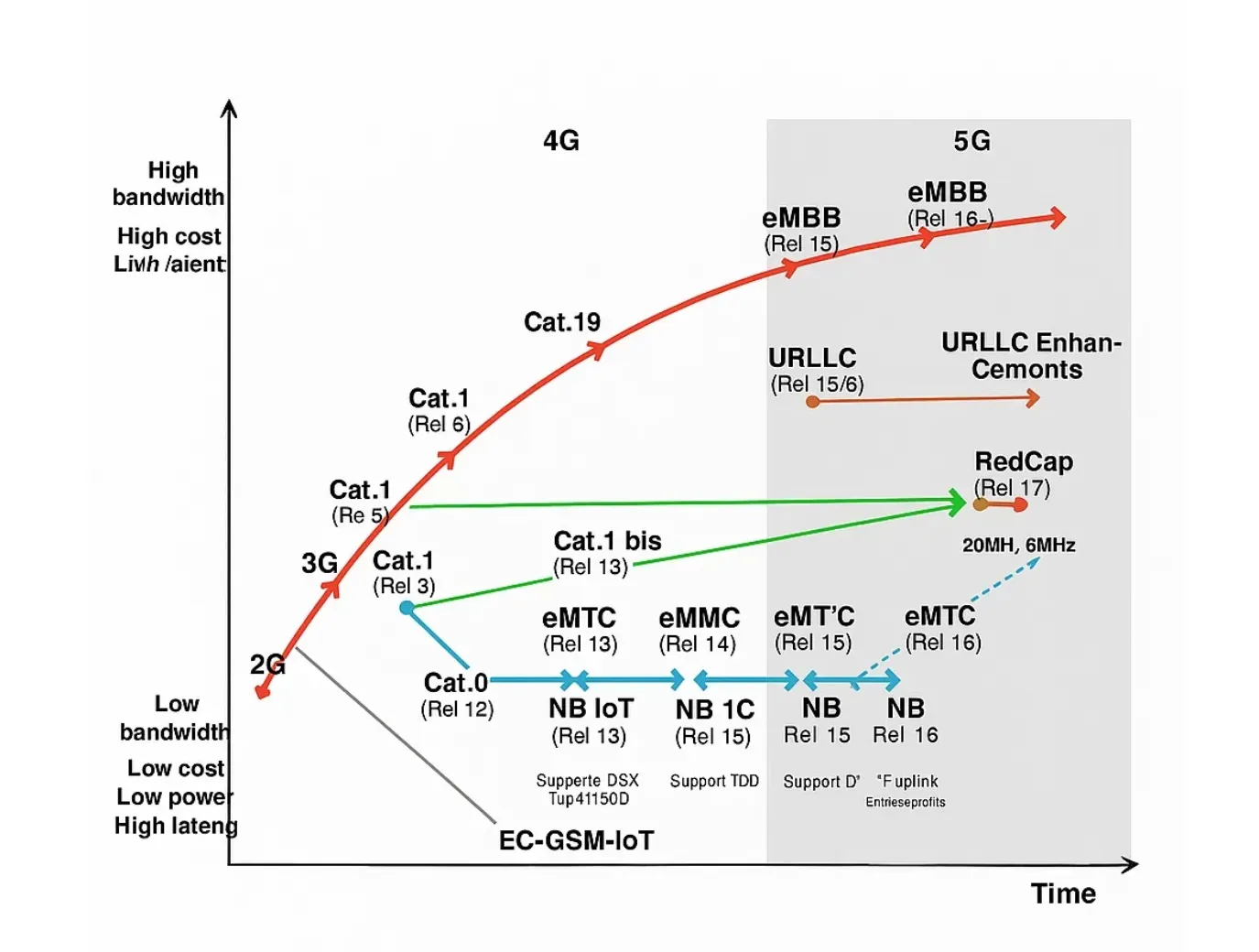
PCB advantages and challenges in RedCap designs:
- Simplified RF Front-End: Fewer MIMO layers and narrower bandwidths allow reduced layer counts and less demanding material specifications, though tight impedance control remains essential for reliable connectivity.
- Lower Power Consumption: Optimized layouts with efficient decoupling and sleep-mode support extend battery life in industrial sensors and wearables.
- Miniaturization via HDI: High-density interconnect with microvias enables small form factor boards while maintaining necessary isolation for stable operation in harsh environments.
- Reliability Focus: High-Tg FR4 or hybrid materials combined with enhanced thermal vias ensure long-term stability in always-on IoT deployments.
VoNR: Voice Services and Signal Integrity in 5G-Only Networks
Voice over New Radio (VoNR) delivers high-quality voice without fallback to 4G, requiring seamless integration of IMS signaling and media processing directly on 5G.
PCB-level implications:
- Low-Latency Audio Paths: Short, impedance-matched traces between baseband processors and audio codecs to minimize delay and jitter.
- RF Chain Stability: Excellent isolation between voice and data paths to prevent packet loss or quality degradation during simultaneous high-speed data transmission.
- Power Efficiency: Advanced power management IC layouts that support rapid transitions between voice and data states without compromising battery performance.
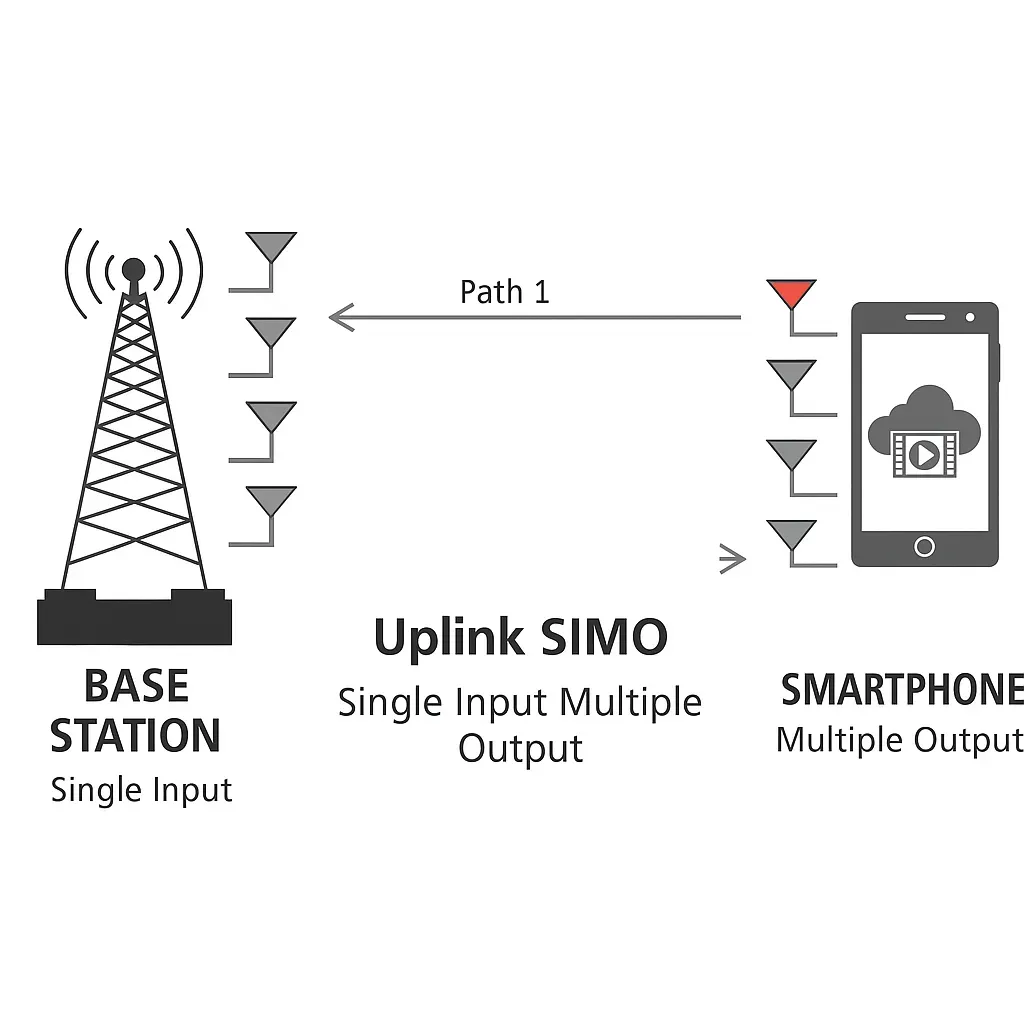
Super Uplink: Enhancing Uplink Performance and PCB Power Handling
Super Uplink aggregates resources across bands and time slots to dramatically boost uplink speeds, particularly valuable for industrial uploads and video surveillance.
This technology stresses PCB designs through:
- Higher Uplink Power Amplifiers: Heavier copper thickness (2oz+) and optimized thermal management solutions, including copper pours and microvia arrays, to handle increased transmit power without overheating.
- Complex Carrier Aggregation Routing: Precise phase matching and isolation between multiple uplink paths to maintain signal quality.
- Dynamic Power Control: Sophisticated PDN designs supporting fast envelope tracking and voltage scaling.
Transport Technologies: OTN vs FlexE in 5G Slicing
For network slicing transport, Optical Transport Network (OTN) provides deterministic, low-latency performance with strong OAM capabilities, while FlexE offers flexible Ethernet-based slicing with lower cost and easier scaling.
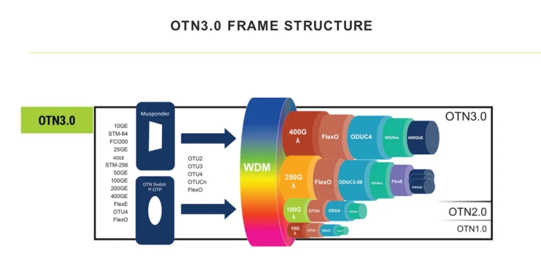
PCB implications for fronthaul/midhaul/backhaul interfaces:
- High-Speed Ethernet Interfaces: 25G/50G/100G SerDes routing with back-drilling and low-loss materials to support both OTN and FlexE protocols.
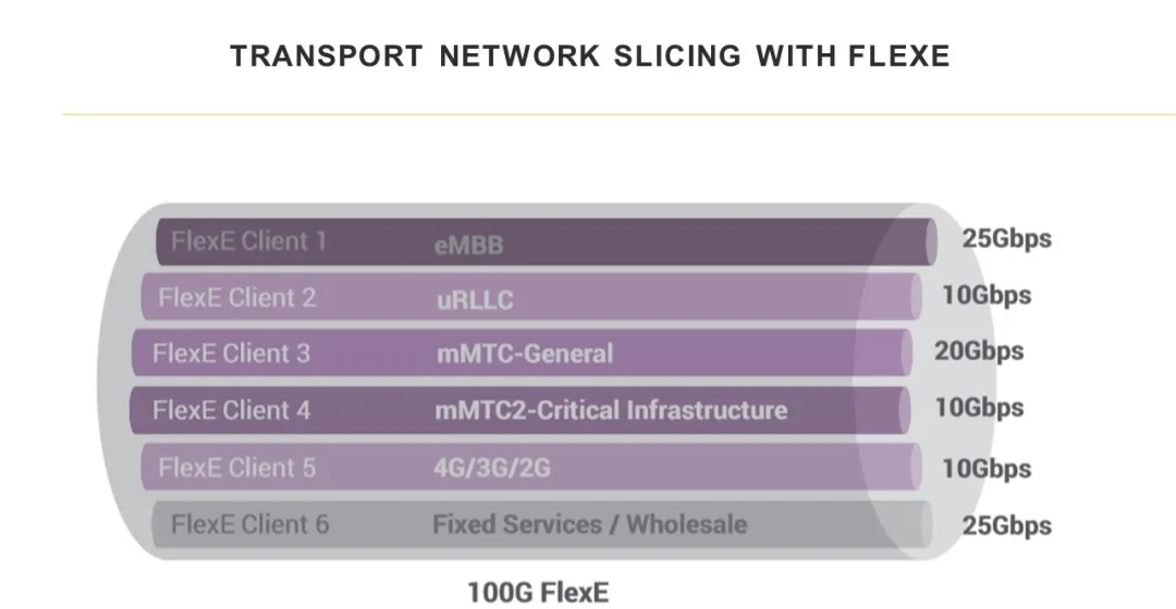
- Timing Synchronization: Ultra-low jitter clock networks essential for precise synchronization across sliced networks.
- Hybrid Board Designs: Support for both optical module interfaces and Ethernet PHYs on the same PCB with excellent EMI control.
5G Messaging and Enhanced Services
Advanced 5G messaging goes beyond SMS with rich media, location services, and IoT coordination. These services require reliable, low-latency data paths.

PCB contributions include:
- Efficient Protocol Processing: Optimized baseband memory interfaces and clean power delivery for real-time messaging applications.
- RF Reliability: Strong signal integrity to ensure consistent delivery even in challenging coverage conditions.
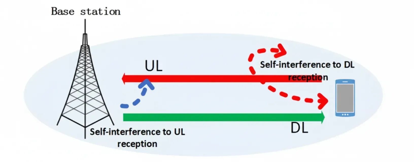
5.5G Evolution and Full Duplex Technology
5.5G (5G-Advanced) bridges 5G and 6G with enhancements in full duplex communication, extended MIMO, and AI-native networking. Full duplex allows simultaneous transmit and receive on the same frequency, doubling spectral efficiency.
PCB challenges in 5.5G and full duplex include:
- Self-Interference Cancellation: Advanced analog and digital cancellation circuits requiring exceptional isolation through multilayer ground planes and via stitching.
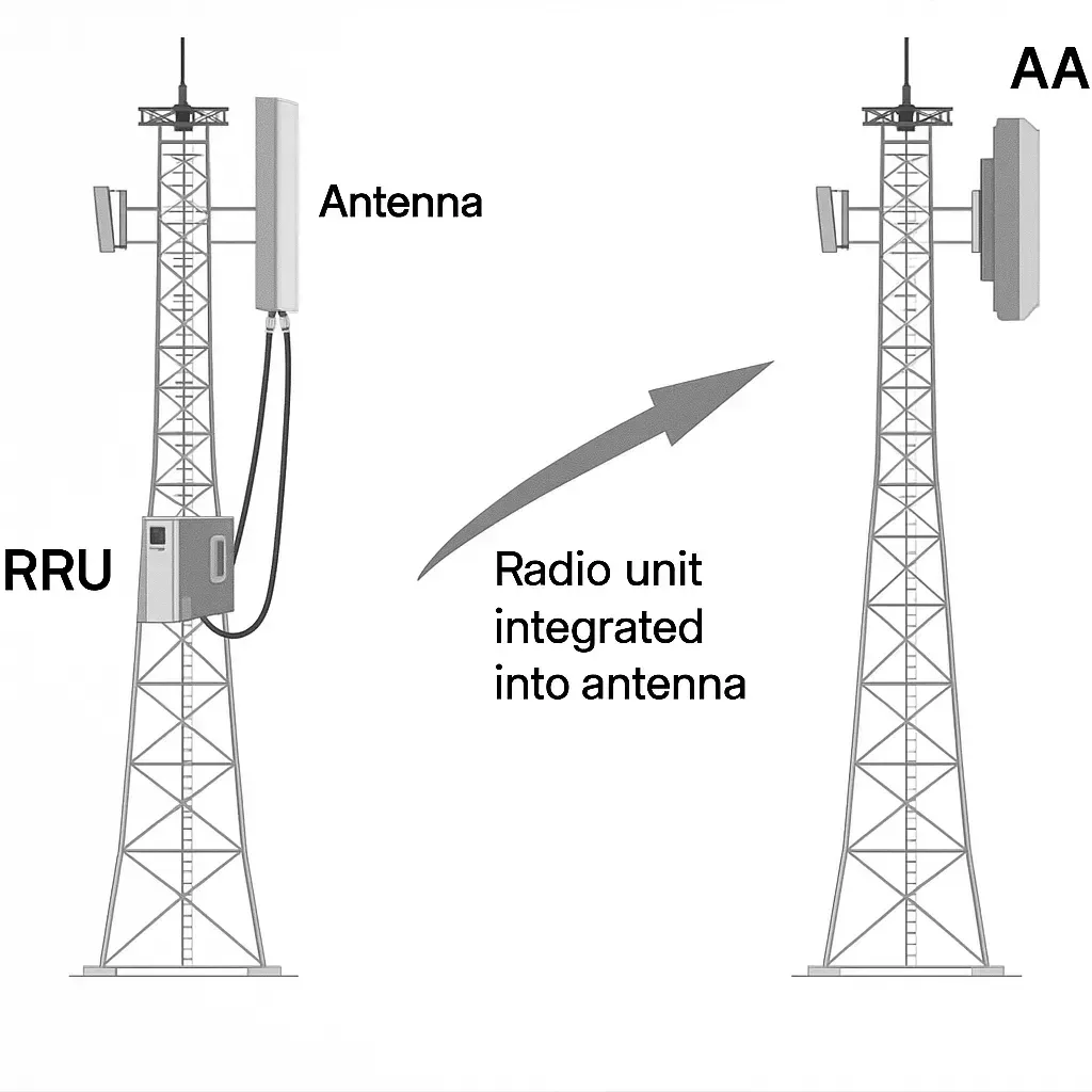
- Massive Antenna Support: Complex HDI stack-ups to route hundreds of antenna elements with minimal crosstalk.
- Higher Processing Density: Increased thermal demands addressed through metal-core or embedded cooling solutions.
- Future-Proof Materials: Low-loss laminates and hybrid constructions that support evolving frequency bands and bandwidths.
PCB Manufacturing Strategies for 5G Advanced Success
To realize these technologies effectively, Aivon delivers:
- Hybrid material stack-ups combining high-frequency laminates for RF with cost-effective cores for digital sections.
- Tight impedance control and advanced via technologies (stacked, blind, buried).
- Comprehensive thermal and signal integrity validation.
- Scalable production supporting both high-volume consumer devices and specialized base station/industrial boards.
- Enhanced reliability features for mission-critical applications in automotive, smart manufacturing, and telecom infrastructure.
The success of network slicing, RedCap, VoNR, Super Uplink, and 5.5G capabilities ultimately depends on excellence in PCB engineering. As 5G networks grow more sophisticated, superior design, material selection, and manufacturing precision become essential differentiators for performance, power efficiency, and reliability.
Aivon provides the advanced PCB solutions required to bring these 5G Advanced technologies from concept to reliable, large-scale deployment.