5G Small Cell Base Station Technology and PCB Integration
Small 5G base stations, often called small cells, play a critical role in delivering high-capacity, low-latency coverage in urban, indoor, and high-traffic environments. Unlike traditional macro base stations, small cells are compact, power-efficient systems where the printed circuit board (PCB) serves as the foundational platform integrating RF front-ends, baseband processing, power management, and antenna interfaces. At Aivon, we specialize in advanced PCBs that enable reliable, high-performance 5G small cell deployments through optimized signal integrity, thermal management, and multilayer manufacturing techniques.
What Defines a Small 5G Base Station
Small 5G base stations are low-power radio access nodes typically outputting between 100mW to 5W, with coverage ranges from 10 meters to 1-2 kilometers. They support both sub-6 GHz and mmWave frequencies and are designed for dense network topologies.
From a PCB perspective, these systems demand:
- Compact Multilayer Designs: HDI PCBs with microvias to accommodate massive MIMO antenna arrays and complex RF chains in limited form factors.
- Hybrid Stack-Ups: Combining standard FR4 with high-frequency, low-loss laminates (such as Rogers or Megtron) for RF layers while maintaining cost-effective digital sections.
- Integrated Power Amplifiers and Filters: Precise impedance control (+/- 5%) for 50 ohm transmission lines to minimize insertion loss and reflections at GHz frequencies.
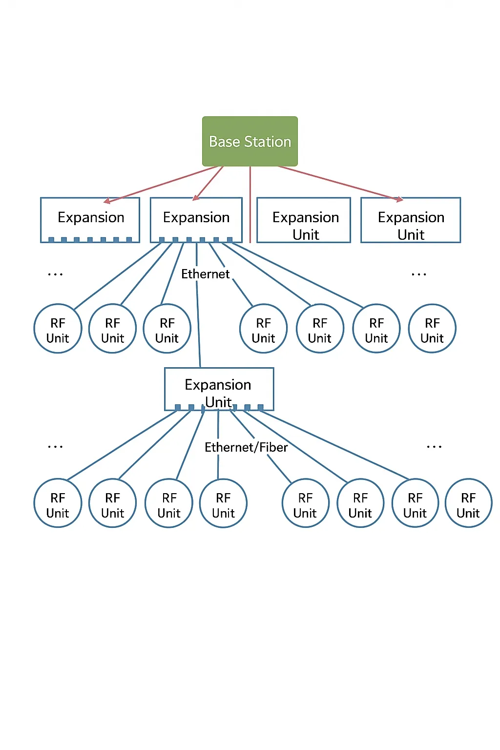
Cell and Sector Relationships in Small Cell Architecture
A single base station can serve one or multiple cells, with each cell potentially divided into sectors using directional antennas. In small cell deployments, this relationship becomes more granular to maximize frequency reuse and capacity.
PCB-level implications include:
- Multi-Channel RF Routing: Separate transmit/receive paths for different sectors require excellent isolation through ground plane stitching, via fences, and careful layer assignment to prevent inter-sector interference.
- Beamforming Support: Digital and hybrid beamforming in 5G small cells relies on synchronized high-speed data buses and low-jitter clock distribution across the PCB.
- Scalable Designs: Modular PCB architectures that allow easy expansion of sectors without compromising signal integrity.
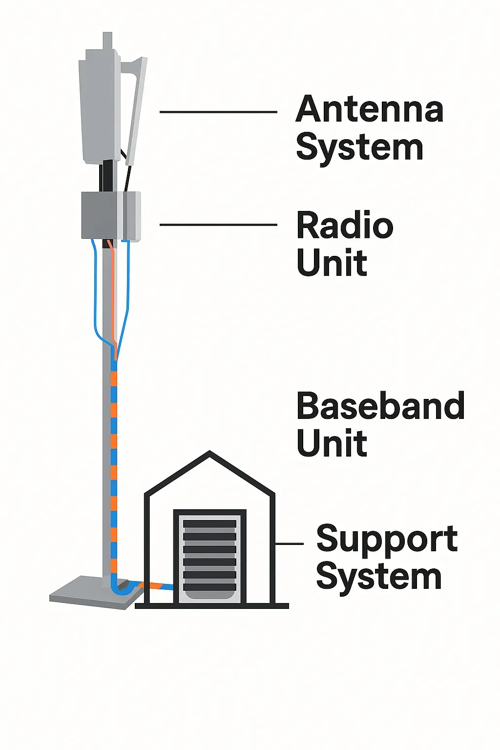
How 5G Base Station Signals Are Transmitted
Signal transmission in 5G small cells utilizes advanced waveforms such as OFDM with massive MIMO and beamforming. The baseband unit processes data before passing it to the radio unit for upconversion and amplification.

Critical PCB design considerations for signal transmission:
- High-Speed Serial Interfaces: Clean routing for CPRI/eCPRI or Ethernet-based fronthaul with controlled impedance and minimal crosstalk.
- RF Chain Optimization: Low-noise power distribution to PAs and LNAs, using heavy copper layers (2oz or higher) for high-current paths and thermal vias for heat dissipation.
- EMI/EMC Management: Strategic component placement and shielding to maintain spectral purity and prevent self-desense in compact enclosures.
Installation Methods for 5G Small Cells
Small cells are deployed on street poles, building facades, lamp posts, and indoor ceilings. This flexibility requires rugged, weatherproof PCB assemblies.
Manufacturing and design adaptations include:
- Conformal Coating and Ruggedization: Enhanced protection against moisture, vibration, and temperature extremes through specialized surface finishes and material selection.
- Thermal Design for Outdoor Use: Advanced thermal management solutions such as metal-core PCBs or integrated heat sinks with microvia arrays to handle solar loading and high ambient temperatures.
- Power Efficiency Focus: Designs optimized for Power over Ethernet (PoE) or direct DC feed, with efficient PDN layouts to minimize voltage drops.
Distributed Small Cell Network Structure and Benefits
Distributed small cell networks consist of multiple low-power nodes coordinated by a central controller, creating a dense heterogeneous network (HetNet) with macro cells.
PCB advantages in this architecture:
- Modular and Scalable Boards: Standardized interfaces that support daisy-chaining or star topologies while maintaining timing synchronization.
- Edge Computing Integration: Baseband PCBs that incorporate local processing to reduce latency for URLLC applications.
- Improved Capacity and Coverage: By reducing cell size, each small cell PCB can focus on high spectral efficiency within its limited area, enabled by superior isolation and filtering.
Key benefits include higher data rates, better user experience in crowded areas, and more efficient spectrum utilization - all underpinned by reliable PCB performance.
Low-Power Design Strategies for 5G Base Stations
Power consumption remains one of the biggest challenges for dense small cell deployments. Effective low-power strategies start at the PCB level:
- Advanced Power Management IC Integration: Optimized layouts with multiple power domains, extensive decoupling, and dynamic voltage scaling support.
- Efficient RF Components: PCB designs that maximize PA efficiency through precise matching networks and harmonic filtering.
- Sleep Mode and Scheduling Support: Fast power state transitions requiring stable power integrity and minimal parasitic inductance in the PDN.
- Material and Process Choices: High-Tg laminates and low-loss dielectrics that reduce dielectric heating, combined with heavy copper for lower resistive losses.
These techniques can significantly reduce overall energy consumption while maintaining peak 5G performance.
PCB Manufacturing Solutions for Small 5G Base Stations
Aivon delivers specialized manufacturing capabilities tailored to small cell requirements:
- Tight impedance control and back-drilling for high-speed signals
- Hybrid material lamination for mixed RF/digital boards
- Advanced via technologies including stacked and filled microvias
- Comprehensive testing for RF performance, thermal cycling, and reliability
- Support for both low-volume prototyping and high-volume production
As 5G networks continue to densify, the performance of small base stations will increasingly depend on excellence in PCB engineering. From signal integrity in complex RF front-ends to thermal reliability in outdoor deployments, superior PCB design and manufacturing directly translate to better network coverage, lower operating costs, and future-proof infrastructure.
Aivon partners with telecom equipment manufacturers to create the high-reliability PCBs that power the next generation of compact, efficient 5G small cell solutions.