Why Thoughtful USB Interface Design is Crucial for Data Reliability
USB interfaces are ubiquitous, connecting everything from personal electronics to industrial systems and IoT devices. They serve as a universal conduit for data exchange, often at high speeds. However, a poorly conceived PCB design can lead to significant problems such as signal degradation, data corruption, or even system malfunctions. Issues like mismatched impedance or unwanted signal reflections can severely disrupt communication.
By meticulously addressing key design elements, including careful trace routing and appropriate connector selection, designers can preempt these common pitfalls. A focused approach ensures consistent and dependable performance for any USB application. This guide will delve into each critical aspect of USB PCB design, providing practical advice and specific recommendations for achieving successful outcomes.
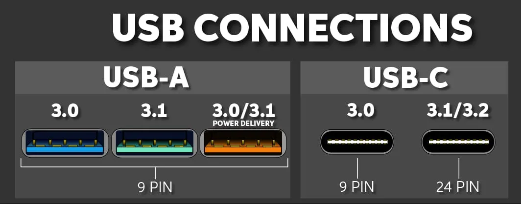
What Are the Key Design Requirements for Different USB Standards?
Before initiating your PCB layout, it's essential to identify the specific USB standard your project will utilize. Each version comes with distinct demands concerning data transfer rates and signal integrity.
Understanding USB 2.0 Design Considerations
USB 2.0 supports data rates up to 480 Mbps. Its data transmission relies on a differential pair (D+ and D-). For this standard, precise impedance control is critical, typically targeting a differential impedance of around 90 ohms.
Design Requirements for USB 3.0/3.1 and USB-C
USB 3.0 (and 3.1) significantly increases speed, offering up to 5 Gbps (Gen 1) or 10 Gbps (Gen 2). These versions introduce additional differential pairs for "SuperSpeed" data, demanding even stricter impedance matching and much shorter trace lengths. The USB-C connector is highly versatile, accommodating USB 2.0, 3.0, and even faster protocols like Thunderbolt. Its compact form factor and high-speed capabilities necessitate exceptionally precise routing. The chosen USB standard will fundamentally influence decisions regarding PCB stackup, trace dimensions, and overall layout.
Related Reading: Integrating USB-C into PCBs: Essential Design Practices
How Does USB Trace Impedance Affect Signal Integrity?
Maintaining accurate trace impedance is arguably the most vital element in USB PCB design. Inconsistencies in impedance along the signal path can generate signal reflections, which in turn cause data errors or a reduction in transfer speeds. For USB interfaces, the differential impedance of the D+ and D- lines should ideally be 90 ohms (with a ±10% tolerance for USB 2.0), with even tighter tolerances required for higher-speed standards like USB 3.0.
Achieving Correct Impedance through Design Parameters
To meet these impedance targets, several design factors must be carefully managed:
● Trace Dimensions: Utilize a PCB impedance calculator to precisely determine the required width and spacing of your differential traces. These calculations depend on the board’s dielectric material properties and thickness. For instance, on a standard FR-4 board with a dielectric constant of 4.2, an 8-mil trace width and 6-mil spacing might yield a 90-ohm differential pair on a two-layer board.
● Layer Stackup: For high-speed USB applications (USB 3.0 and beyond), a four-layer or more complex stackup is highly recommended. Signal traces are typically placed on the top layer, directly above a solid ground plane, which helps control impedance and effectively mitigates noise.
● Material Selection: The chosen PCB substrate directly influences impedance characteristics. While standard FR-4 is generally sufficient for USB 2.0, advanced low-loss materials should be considered for USB 3.0 and faster versions to minimize signal attenuation.
By meticulously controlling USB trace impedance, designers establish a robust foundation for dependable data transfer across the interface.
What Are the Best Practices for Routing USB Differential Pairs?
USB data lines function as differential pairs, meaning the D+ and D- signals are transmitted in tandem and require meticulous routing. Correct differential pair routing is essential for ensuring both traces experience an identical electrical environment, thereby minimizing noise ingress and signal skew.
Essential Guidelines for Routing Differential Pairs
Consider these best practices when laying out differential pairs:
● Length Matching: Strive to keep the D+ and D- trace lengths as precisely equal as possible. For USB 2.0, a length variance of less than 150 mils is typically acceptable, but for USB 3.0, aim for a discrepancy under 15 mils to prevent timing issues at elevated speeds.
● Consistent Spacing: Maintain a uniform distance between the two traces throughout their entire length to preserve consistent impedance. Avoid abrupt changes in spacing or routing these pairs close to other high-speed signals.
● Via Minimization: Limit the use of vias on differential pairs as much as possible, as each via introduces an impedance discontinuity. If vias are unavoidable, employ back-drilling techniques or ensure they are placed symmetrically for both traces.
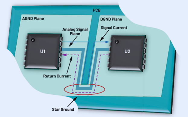
● Continuous Ground Plane: Route differential pairs over an unbroken ground plane. This practice helps to suppress electromagnetic interference (EMI) and provides a stable, low-impedance return path for signals.
Adhering to these guidelines is crucial for preserving signal integrity, particularly at higher data rates.
Related Reading: USB-C Integration on PCBs: A Design Guide for Engineers
How Do I Select the Right USB Connector for My Design?
The choice of USB connector is as vital as the trace routing itself, influencing both the physical connection and the overall signal quality and durability of the interface. With numerous options available—such as Type-A, Type-B, Micro-USB, and USB-C—your selection should align with the specific application and the targeted USB standard.
Key Considerations for Connector Selection
When choosing a USB connector, keep the following factors in mind:
● USB Version Compatibility: Confirm that the connector fully supports the USB standard you intend to use. For instance, USB-C connectors are highly versatile for modern designs, offering support for USB 2.0, 3.0, and newer standards, along with reversible plug orientation.
● Physical Footprint: For devices with limited space, compact connectors like Micro-USB or USB-C are ideal. In industrial environments where robustness is key, sturdier options like Type-A or Type-B might be more appropriate.
● Durability Rating: Evaluate the connector's mating cycle rating, which indicates its expected lifespan under repeated insertions. USB-C connectors often boast ratings up to 10,000 cycles, making them highly durable for frequent use.
● Signal Pin Requirements: Higher-speed standards, such as USB 3.0, necessitate additional pins for their SuperSpeed data lines. Verify that the selected connector accommodates all the necessary signals for your specific design.
A thoughtfully chosen connector guarantees a reliable physical and electrical connection, significantly reducing the likelihood of data transfer problems.
What Strategies Minimize Signal Reflections in USB Designs?
Signal reflections occur when there is an impedance mismatch along the signal path, causing a portion of the transmitted signal to bounce back and interfere with the original signal. Minimizing these reflections is critical for maintaining data integrity in USB interfaces, especially at high speeds.
Techniques to Reduce Signal Reflections
Here’s how to effectively manage and reduce signal reflections:
● Consistent Impedance: Ensure that the USB trace impedance remains uniform throughout the entire signal path. This includes the traces, vias, and connections to components and the connector. Any abrupt change can act as a reflection point.
● Termination Schemes: For USB 2.0, the host and device typically incorporate internal termination. However, in custom designs or for higher-speed standards, verify that appropriate termination resistors are correctly implemented as required by the specific chipset or standard.
● Smooth Trace Bends: Route traces with gradual, smooth bends (using 45-degree angles or gentle curves) rather than sharp 90-degree turns. Sharp corners can introduce localized impedance changes, leading to reflections.
● Optimal Connector Placement: Position the USB connector as close as possible to the USB controller integrated circuit (IC). This minimizes trace length, thereby reducing the number of potential reflection points and overall signal degradation.
By proactively addressing these aspects, you can significantly diminish signal reflections and enhance the overall performance and reliability of your USB interface.
What Are the Best Practices for USB PCB Layout?
An expertly designed USB PCB layout integrates all the previously discussed elements into a cohesive whole. The layout directly influences signal integrity, the level of noise, and electromagnetic interference (EMI). Adhering to specific best practices is essential for creating an effective and robust USB PCB layout.
Key Elements of an Effective USB PCB Layout
Follow these guidelines to optimize your PCB layout for USB interfaces:
● Minimize Trace Lengths: Keep USB data traces as short as possible. Shorter traces reduce signal delay, attenuation, and the likelihood of picking up noise. For USB 3.0, trace lengths should ideally not exceed 4 inches.
● Dedicated Power and Ground Planes: Allocate separate, stable layers or areas specifically for the power supply (Vbus) and ground. This provides a consistent voltage source and a low-impedance return path for signals. Place decoupling capacitors (e.g., 0.1 μF and 1 μF) in close proximity to the USB controller IC to effectively filter out high-frequency noise.
● Isolation from Noise Sources: Route USB traces away from potential sources of high-frequency noise, such as switching regulators, clock generators, or power amplifiers. This isolation helps prevent crosstalk and maintains signal integrity.
● Robust Shielding and Grounding: For USB connectors, ensure that the metal shield is properly grounded to the PCB. Connect the shield to the ground plane using multiple vias. This robust grounding minimizes EMI radiation and improves the immunity of the interface to external noise.
A clean, well-organized USB PCB layout significantly reduces potential issues, contributing to consistently reliable data transfer.
Suggested Reading: Enhancing USB Performance: A Guide to Optimal PCB Layout and Signal Integrity
Overcoming Common Challenges in USB PCB Design
Despite careful planning, designing USB PCBs can present various challenges. Anticipating these issues and having solutions ready can streamline the development process.
Addressing Common USB Design Hurdles
Here are some frequent problems encountered and practical ways to overcome them:
● EMI Interference: High-speed USB signals are susceptible to, and can generate, electromagnetic interference. Mitigate this by implementing effective shielding, ensuring proper grounding, and incorporating ferrite beads on power lines to filter noise.
● Space Constraints: In compact device designs, accommodating USB traces and connectors can be difficult. Prioritize short, direct routing paths and consider using smaller form-factor connectors like USB-C to conserve board space.
● Signal Skew: Mismatched trace lengths within differential pairs are a primary cause of signal skew. Utilize advanced PCB design software features that offer length-matching tools to ensure traces are kept as equal as possible.
Proactively tackling these challenges early in the design cycle can prevent costly revisions and delays in the project timeline.
Testing and Validating Your USB PCB Design for Reliability
Once your PCB is designed and manufactured, comprehensive testing is indispensable to confirm that it facilitates reliable data transfer. This validation phase ensures the design meets performance specifications and functions as intended in real-world scenarios.
Essential Methods for Design Validation
Employ these key testing methods to thoroughly evaluate your USB PCB design:
● Signal Integrity Analysis: Use a high-bandwidth oscilloscope to meticulously inspect the USB data lines for any signs of signal reflections, jitter, or unwanted noise. Crucially, verify that the eye diagram generated from the signals meets the specific requirements outlined in the USB specification for your chosen standard.
● Impedance Verification: Employ a time-domain reflectometer (TDR) to accurately measure the differential impedance of your traces. Confirm that these measurements precisely match your target impedance (e.g., 90 ohms for USB 2.0).
● Functional Compatibility Testing: Connect your developed device to a diverse range of USB hosts and peripheral devices. This helps confirm expected data transfer rates, ensures broad compatibility, and validates overall operational performance across various scenarios.
Rigorous testing helps identify and rectify potential issues before they reach end-users, ensuring the delivery of a high-quality, dependable product.
Crafting Reliable USB Interfaces Through Optimal PCB Design
Developing a PCB for USB interfaces demands meticulous attention to detail. This ranges from precisely controlling USB trace impedance and executing accurate differential pair routing to selecting appropriate connectors, minimizing signal reflections, and optimizing the overall USB PCB layout. By adhering to the comprehensive guidelines and best practices outlined in this guide, engineers can create designs that guarantee reliable data transfer across a multitude of applications.
Begin with a clear understanding of the specific USB standard relevant to your project. Then, shift your focus to rigorous impedance control, precise trace routing, and judicious component selection. With a well-conceived layout and thorough testing, your USB interface will consistently deliver robust performance, whether it’s integrated into a consumer gadget or a complex industrial system.
At AIVON, we are dedicated to providing engineers with the essential tools and resources needed for successful PCB designs. By applying these fundamental principles to your next project, you will be well-equipped to engineer highly robust and efficient USB interfaces