Introduction
Wave soldering machines play a critical role in the assembly of printed circuit boards, particularly for through-hole components. This automated soldering process is widely used in high-volume production environments where speed and consistency are essential. For electrical engineers, understanding the pros and cons of wave soldering is vital for making informed decisions about assembly methods. This article explores the benefits of wave solder, such as efficiency and cost-effectiveness, alongside drawbacks like design limitations and potential quality issues. By examining when to use wave solder, engineers can better align their project needs with the right technology. The discussion will provide practical insights into optimizing the use of wave soldering machines while adhering to industry standards for quality and performance.
What Is Wave Soldering and Why It Matters
Wave soldering is a bulk soldering technique used in PCB assembly to bond through-hole components to the board. It involves passing the PCB over a molten solder wave, which contacts the underside of the board, creating reliable joints between component leads and pads. This method is especially significant for projects requiring rapid production of assemblies with through-hole parts, as it can handle large batches efficiently.
The importance of wave soldering lies in its ability to streamline manufacturing processes in industries like consumer electronics, automotive, and industrial equipment. For electrical engineers, selecting the appropriate soldering method impacts production timelines, costs, and product reliability. Wave soldering offers a balance between speed and quality for specific applications, making it a key consideration during design and assembly planning. Understanding its strengths and limitations ensures better decision-making for optimal outcomes.
Technical Principles of Wave Soldering Machines
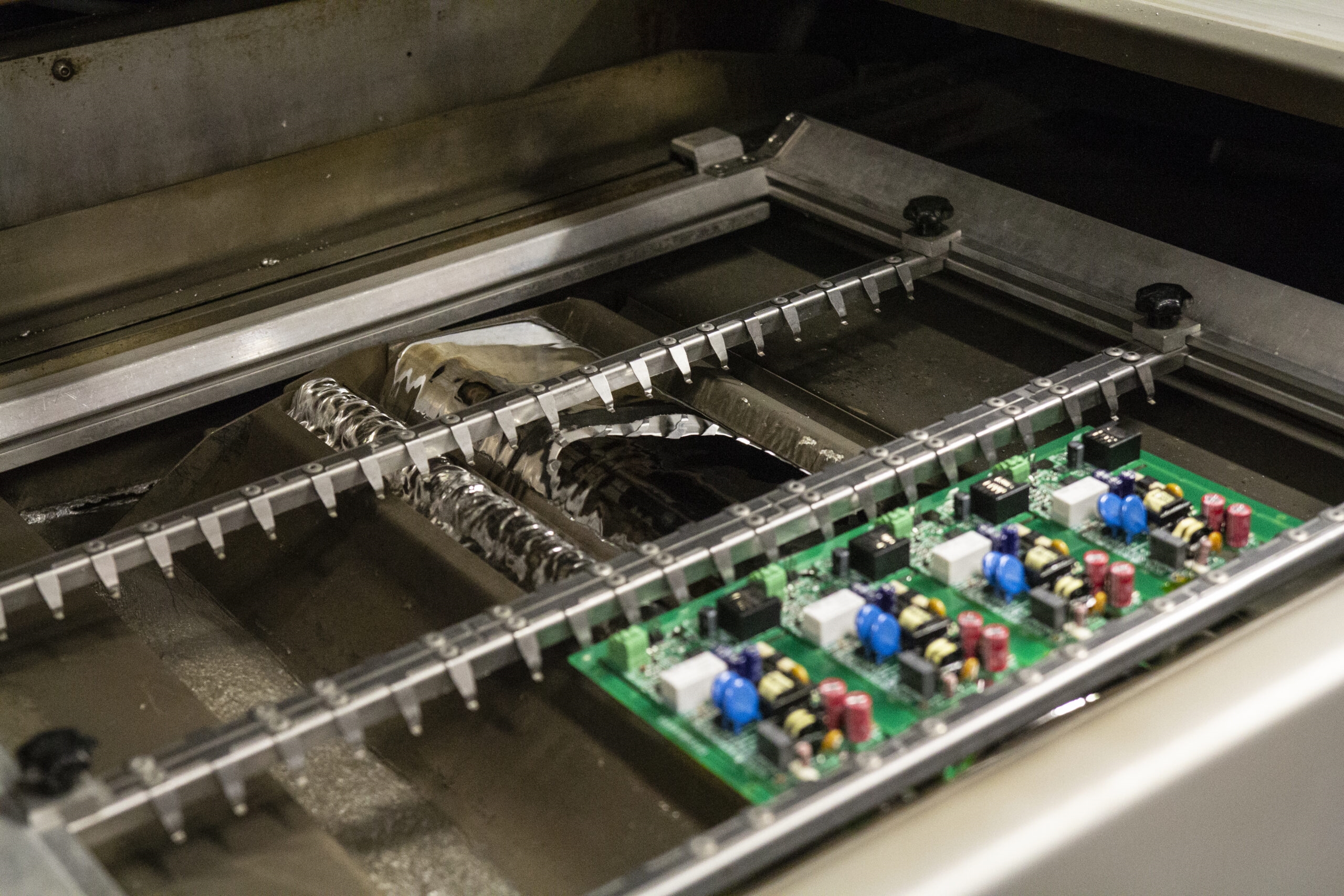
Wave soldering operates on a straightforward yet precise mechanism. The process begins with the application of flux to the PCB to clean surfaces and enhance solder adhesion. The board then passes through a preheating stage to activate the flux and reduce thermal shock to components. Following this, the PCB moves over a wave of molten solder, typically maintained at a controlled temperature as per industry guidelines like those in IPC J-STD-001H. The solder wave contacts exposed metal areas, forming joints as the board exits the wave and cools.
The machine's design includes a solder pot, pump system to generate the wave, and conveyor to transport PCBs. Flux application and preheating zones are integrated to ensure consistent results. This automated setup minimizes human error, but it requires careful calibration to avoid issues like solder bridging or insufficient wetting. Engineers must consider component placement and board layout to ensure compatibility with the wave soldering process, as tight spacing or mixed technology designs can pose challenges.
Advantages of Wave Soldering Machines
Wave soldering offers several benefits that make it a preferred choice for specific PCB assembly scenarios. Below are the key advantages, particularly relevant for electrical engineers focusing on production efficiency and reliability.
- High Throughput for Mass Production: Wave soldering excels in high-volume manufacturing. It can process multiple boards quickly, making it ideal for projects with consistent through-hole component designs. This speed is a key differentiator in the wave soldering vs. hand soldering decision, significantly reducing production time.
- Cost-Effectiveness in Bulk: The automated nature of wave soldering lowers labor costs in large-scale operations. Once set up, the machine requires minimal intervention, providing economies of scale for repetitive tasks.
- Reliable Joint Formation: When executed under controlled conditions, wave soldering produces strong, uniform solder joints for through-hole components. Standards like IPC-A-600K emphasize the importance of consistent joint quality, which wave soldering can achieve with proper setup.
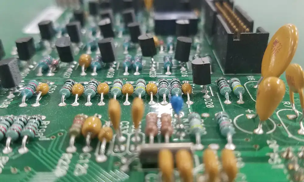
- Simplified Process for Through-Hole Parts: Unlike surface-mount technology processes, wave soldering is specifically tailored for through-hole components, ensuring effective bonding without complex adjustments for varied component types.
Disadvantages of Wave Soldering Machines
Despite its advantages, wave soldering comes with notable drawbacks that engineers must evaluate before implementation. Understanding these limitations helps in determining when to use wave solder and when alternative methods might be more suitable.
- Limited Compatibility with SMT Designs: Wave soldering is primarily designed for through-hole components. Surface-mount technology parts on the underside of the board can be damaged by the solder wave or require additional masking, increasing complexity and cost.
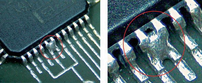
- Risk of Solder Bridging and Defects: Improper setup or board design can lead to solder bridging between closely spaced leads, causing short circuits. Adhering to design guidelines in IPC-2221B can mitigate this, but it requires meticulous planning.
- Thermal Stress on Components: The exposure to high temperatures during the soldering wave can stress certain components, potentially leading to failures. Preheating helps, but sensitive parts may still be at risk.
- Higher Maintenance Needs: Wave soldering machines require regular maintenance to prevent solder contamination and ensure wave consistency. Flux residues and dross buildup can affect performance if not addressed promptly.
- Design Constraints for Mixed Assemblies: For boards with both through-hole and surface-mount components, wave soldering often necessitates secondary processes like reflow soldering, adding to production time and cost.
For more advantages of wave soldering, see our PCB Soldering guide: The Definitive Guide to PCB Soldering: Standards, Techniques, and Strategic Implementation
When to Use Wave Soldering Machines
Determining when to use wave solder involves assessing the specific needs of a project. This method is most effective under certain conditions, which electrical engineers should evaluate during the planning phase.
- High-Volume Through-Hole Assemblies: Wave soldering is ideal for projects with large quantities of through-hole components. Its ability to handle bulk production makes it suitable for applications like power supplies or industrial control boards.
- Cost-Sensitive Production: When budget constraints are a priority, wave soldering offers a cost-effective solution for repetitive tasks. It minimizes labor costs and maximizes output in such scenarios.
- Simple Board Designs: Boards with straightforward layouts and minimal component density are well-suited for wave soldering. Complex designs with tight spacing may encounter issues like bridging or incomplete soldering.
- Legacy Designs: Older PCB designs often rely on through-hole technology. Wave soldering remains a practical choice for maintaining consistency in manufacturing these legacy products without redesigning for surface-mount processes.
Conversely, wave soldering may not be appropriate for mixed-technology boards or designs with heat-sensitive components In such cases, engineers might consult a guide to selective soldering or consider reflow methods to avoid the limitations associated with wave soldering. Adhering to standards like IPC J-STD-001H ensures that the chosen method meets quality and reliability expectations.
Best Practices for Optimizing Wave Soldering
To maximize the benefits of wave solder while minimizing its drawbacks, electrical engineers can follow several best practices. These actionable steps ensure consistent results and reduce the likelihood of defects.
- Optimize Board Layout: Design the PCB with wave soldering in mind. Follow guidelines from IPC-2221B to space components appropriately and orient them to minimize shadowing effects during the solder wave.
- Control Process Parameters: Maintain strict control over solder temperature, wave height, and conveyor speed. Refer to IPC J-STD-001H for acceptable ranges to avoid thermal damage or insufficient soldering.
- Use Quality Flux: Select a flux compatible with the board materials and components. Proper flux application enhances wetting and reduces defects like solder balls or bridging.
- Implement Regular Maintenance: Clean the solder pot and remove dross frequently to prevent contamination. Inspect the wave mechanism to ensure uniform solder flow across the board.
- Test and Inspect: Conduct post-soldering inspections using criteria from IPC-A-600K to identify defects early. Automated optical inspection systems can assist in detecting issues like bridging or insufficient joints.
By adhering to these practices, engineers can address many challenges associated with wave soldering, ensuring reliable outcomes for their projects.
Troubleshooting Common Wave Soldering Issues
Even with best practices, wave soldering can encounter problems that affect quality. Electrical engineers should be prepared to troubleshoot common issues to maintain production efficiency.
- Solder Bridging: Often caused by excessive solder or improper component spacing. Adjust wave height and ensure design compliance with IPC-2221B to prevent this defect.
- Insufficient Solder Joints: This can result from inadequate flux or low preheat temperatures. Verify flux coverage and adjust preheating to activate it effectively before the solder wave.
- Component Damage: Thermal shock may damage sensitive parts. Increase preheat duration to minimize temperature gradients as the board enters the wave.
- Flux Residue: Excessive residue can lead to corrosion over time. Use a no-clean flux if compatible, or ensure thorough cleaning post-soldering per IPC J-STD-001H guidelines.
Addressing these issues promptly ensures that the wave soldering process remains reliable and meets quality standards expected in professional assembly environments.
Conclusion
Wave soldering machines offer a powerful solution for PCB assembly, particularly in high-volume production of through-hole designs. The pros and cons of wave soldering reveal a balance between efficiency and limitations that electrical engineers must navigate. Benefits like cost-effectiveness and speed make it a valuable tool, while drawbacks such as design constraints and potential defects require careful management. Knowing when to use wave solder, alongside adherence to standards like IPC J-STD-001H and IPC-A-600K, enables engineers to optimize outcomes. By implementing best practices and troubleshooting strategies, the challenges of wave soldering can be mitigated, ensuring reliable and consistent results in manufacturing processes.
FAQs
Q1: What are the main benefits of wave solder for PCB assembly?
A1: Wave soldering provides significant advantages for high-volume production. It offers fast processing of through-hole components, reducing assembly time. Cost-effectiveness is another key benefit, as automation lowers labor expenses. When aligned with standards like IPC-A-600K, it ensures consistent solder joint quality, making it a reliable choice for electrical engineers handling large batches of similar designs.
Q2: What are the common drawbacks of wave solder in modern designs?
A2: Wave soldering has limitations, especially with mixed-technology PCBs. It struggles with surface-mount components, risking damage or requiring extra steps. Solder bridging and thermal stress are frequent issues if parameters aren't controlled. Adhering to IPC-2221B for design can help, but engineers must still address maintenance needs and compatibility challenges in complex assemblies.
Q3: When should electrical engineers use wave soldering machines?
A3: Engineers should opt for wave soldering when working on high-volume through-hole assemblies. It suits cost-sensitive projects and simple board layouts where speed is critical. It's less ideal for mixed designs or heat-sensitive parts. Following IPC J-STD-001H ensures quality, helping decide when to use wave solder over alternatives like reflow or selective soldering.
Q4: How can defects in wave soldering be minimized effectively?
A4: Minimizing defects requires strict process control and design optimization. Adjust solder wave parameters and ensure proper preheating per IPC J-STD-001H. Use quality flux and maintain the machine to avoid contamination. Regular inspection against IPC-A-600K criteria helps catch issues like bridging early, ensuring reliable joints in wave soldering applications.
References
IPC J-STD-001H — Requirements for Soldered Electrical and Electronic Assemblies. IPC, 2021.
IPC-A-600K — Acceptability of Printed Boards. IPC, 2020.
IPC-2221B — Generic Standard on Printed Board Design. IPC, 2012.


