Introduction
In the fast-paced world of electronics, producing cost-effective and reliable printed circuit boards (PCBs) is a priority for electrical engineers. Design for Manufacturability (DFM) offers a structured approach to optimize PCB designs, focusing on reducing assembly costs while maintaining quality. By integrating DFM guidelines for PCB cost reduction, engineers can streamline production, minimize errors, and enhance efficiency. This article explores the critical role of DFM in PCB assembly, delving into component placement for assembly cost optimization and strategies for minimizing assembly time. With practical insights and adherence to industry standards, this guide aims to equip professionals with actionable design rules and cost-saving techniques to improve their workflow and output in the competitive electronics landscape.
What Is Design for Manufacturability (DFM) and Why It Matters
Design for Manufacturability (DFM) refers to the practice of designing products in a way that simplifies manufacturing and assembly processes. In the context of PCBs, DFM focuses on creating layouts and selecting components that reduce production complexities, lower costs, and ensure reliability. This approach is vital for electrical engineers as it directly impacts project timelines, budgets, and product quality.
The significance of DFM lies in its ability to bridge the gap between design and production. A poorly designed PCB can lead to assembly delays, increased rework, and higher expenses. By following DFM principles, engineers can avoid common pitfalls such as improper component placement or incompatible materials. Ultimately, DFM guidelines for PCB cost reduction help in achieving a balance between functionality and manufacturability, ensuring that designs are both innovative and practical for large-scale production.
Technical Principles of DFM in PCB Assembly
DFM in PCB assembly revolves around optimizing the design to facilitate efficient manufacturing. Several technical principles underpin this approach, each addressing specific challenges in the assembly process.
First, component selection plays a crucial role. Choosing standard, widely available components reduces procurement costs and lead times. It also minimizes the risk of supply chain disruptions. Engineers must prioritize components that align with industry standards for compatibility and reliability during assembly.
Second, the layout design must consider the assembly equipment capabilities. Automated pick-and-place machines, commonly used in surface mount technology (SMT), require specific spacing and orientation rules for components. Ignoring these can result in placement errors or machine downtime, increasing costs.
Third, minimizing the number of unique components simplifies inventory management and reduces setup times on assembly lines. This principle directly contributes to minimizing assembly time, as fewer changeovers are needed during production.
Lastly, designing for testability ensures that potential defects can be identified early. Incorporating test points and accessible pads in the layout allows for efficient in-circuit testing, reducing debugging time and associated expenses. These principles collectively form the foundation of effective DFM strategies, ensuring cost efficiency without compromising quality.
Related Reading: PCB Prototype Design for Manufacturability (DFM): Avoiding Costly Errors
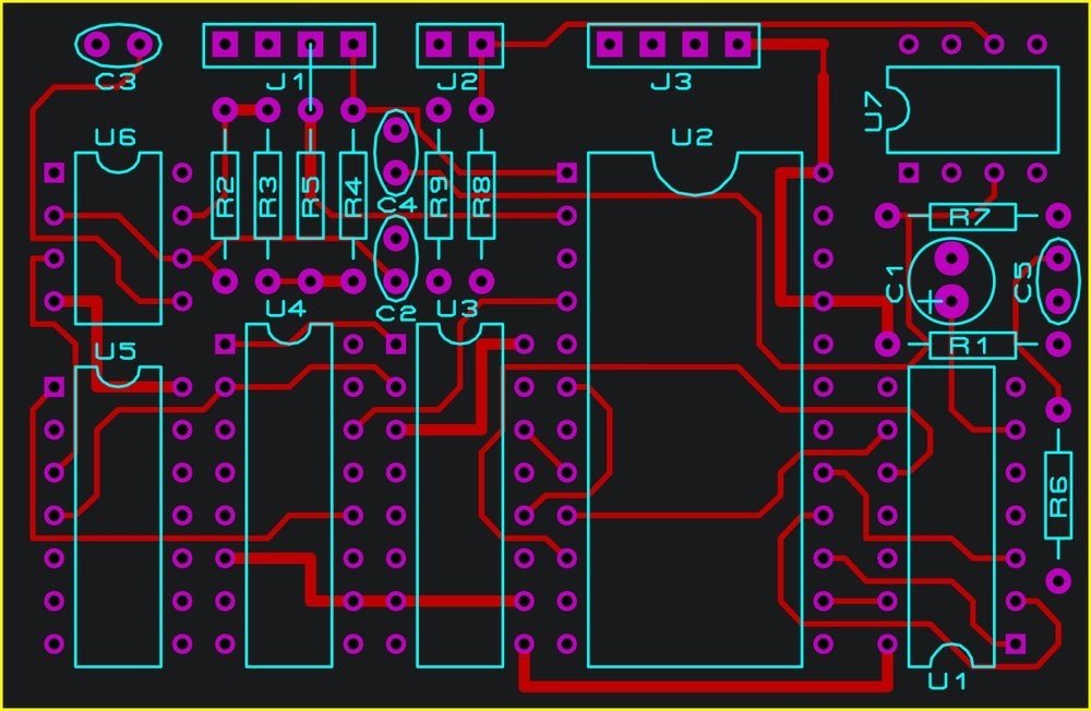
Best Practices for Component Placement in Assembly Cost Reduction
Component placement for assembly cost optimization is a critical aspect of DFM. Proper placement not only speeds up the assembly process but also reduces errors and rework. Below are actionable best practices to achieve these goals.
-
Group Similar Components Together: Place components of the same type or value in clusters. This reduces the number of tool changes in automated assembly, thus minimizing assembly time.
-
Maintain Uniform Orientation: Align components in the same direction whenever possible. Uniform orientation prevents rotation adjustments by pick-and-place machines, enhancing speed and accuracy.
-
Adhere to Spacing Guidelines: Ensure adequate spacing between components to avoid interference during placement or soldering. Overcrowding can lead to defects and necessitate costly manual corrections.
-
Prioritize Single-Sided Assembly: If feasible, place all components on one side of the PCB. This eliminates the need for flipping the board during assembly, cutting down on process steps and associated costs.
-
Position Large Components Strategically: Place larger or heavier components near the center or in areas that minimize stress on the board during handling. This reduces the risk of damage and improves assembly stability.
Following these practices ensures that the assembly process is streamlined, directly impacting design rules and cost efficiency. Additionally, referencing standards like IPC-7351B for land pattern design can guide engineers in achieving optimal component placement.
Related Reading: Designing for Batch Assembly: Best Practices for Component Placement
Strategies for Minimizing Assembly Time
Minimizing assembly time is a core objective of DFM, as it directly correlates with reduced labor costs and faster time-to-market. Implementing the following strategies can significantly enhance assembly efficiency.
First, simplify the design by reducing the number of components. Fewer parts mean less time spent on placement and soldering. Engineers should evaluate if certain functions can be integrated into a single component to achieve this.
Second, avoid complex assembly processes. For instance, using through-hole components alongside SMT parts increases assembly steps, as they require different techniques. Opting for a uniform assembly method, preferably SMT, can save considerable time.
Third, design with automation in mind. Automated assembly lines are faster and more precise than manual methods. Ensuring the PCB layout accommodates automation, such as providing clear fiducial markers for machine alignment, is essential.
Fourth, minimize manual interventions. Designs that require hand soldering or special handling increase assembly time. Incorporating features like self-aligning components or standardized connectors can mitigate this issue.
Lastly, collaborate with manufacturing teams during the design phase. Early feedback on potential assembly bottlenecks allows for adjustments before production begins. These strategies collectively contribute to DFM guidelines for PCB cost reduction, ensuring a smoother and quicker assembly process.
Design Rules and Cost Optimization Insights
Design rules and cost considerations are interlinked in PCB development. Adhering to well-established design rules not only ensures manufacturability but also drives down expenses. Key insights in this area include focusing on standardization and scalability.
Standardization involves using common board sizes, layer counts, and materials that align with industry norms. Deviating from standard specifications often results in higher fabrication costs due to custom setups or specialized equipment needs. Referencing standards like IPC-6012E for rigid PCB performance specifications can help maintain consistency.
Scalability ensures that the design can accommodate future production increases without major rework. Planning for scalability during the initial design phase prevents costly redesigns as demand grows. This includes leaving room for additional components or test points.
Another critical aspect is reducing layer count where possible. Each additional layer increases fabrication complexity and cost. Engineers should strive for minimal layers while meeting performance requirements.
Finally, incorporating error-proofing features, often termed as poka-yoke in manufacturing, prevents assembly mistakes. Simple additions like polarized connectors or unique footprints for similar components can avoid costly errors. These design rules and cost-focused insights are essential for achieving long-term savings in PCB production.
Practical Troubleshooting in DFM Implementation
Implementing DFM principles can sometimes present challenges, especially when balancing cost, performance, and manufacturability. Troubleshooting common issues is a practical skill for electrical engineers to master.
One frequent issue is component misalignment during assembly, often due to incorrect land patterns or insufficient spacing. Reviewing the design against standards like IPC-7351B can help identify and correct such discrepancies before production.
Another challenge is thermal stress during soldering, which can cause component damage or board warpage. Designing with proper thermal relief patterns and ensuring compliance with soldering profiles as outlined in JEDEC J-STD-020E can mitigate these risks.
Lastly, unexpected assembly delays may arise from supply chain issues with non-standard components. Early validation of component availability and opting for alternatives that meet specifications can prevent such disruptions. Addressing these challenges through proactive design adjustments ensures that DFM principles effectively reduce assembly costs.
Conclusion
Design for Manufacturability (DFM) stands as a cornerstone for electrical engineers aiming to reduce PCB component assembly costs. By integrating DFM guidelines for PCB cost reduction, optimizing component placement for assembly cost, and focusing on minimizing assembly time, engineers can achieve significant savings and efficiency. Practical design rules and cost-focused strategies further enhance the manufacturability of PCBs, ensuring they meet both technical and economic goals. Embracing these principles not only streamlines production but also upholds the quality and reliability essential in the electronics industry. Through careful planning and adherence to industry standards, DFM transforms complex designs into cost-effective solutions.
FAQs
Q1: How do DFM guidelines for PCB cost reduction impact production efficiency?
A1: DFM guidelines streamline production by optimizing designs for ease of manufacturing. They reduce assembly errors, minimize rework, and lower material waste. By focusing on standard components and simplified layouts, production becomes faster and more cost-effective. Adhering to these guidelines ensures that designs align with manufacturing capabilities, directly enhancing overall efficiency.
Q2: What role does component placement for assembly cost play in PCB design?
A2: Component placement is critical in reducing assembly costs. Proper placement minimizes machine adjustments, speeds up automated processes, and prevents errors. Grouping similar components and maintaining uniform orientation cuts down setup times. Strategic placement also reduces the risk of defects, ensuring a smoother assembly process with lower expenses.
Q3: How can engineers focus on minimizing assembly time during PCB design?
A3: Engineers can minimize assembly time by simplifying designs with fewer components and uniform assembly methods. Prioritizing automation-friendly layouts and avoiding manual processes helps. Using single-sided assembly and standardized parts further reduces time. Early collaboration with manufacturing teams also identifies potential delays before production starts.
Q4: Why are design rules and cost considerations important in DFM?
A4: Design rules ensure manufacturability while keeping costs in check. Standardized sizes, minimal layers, and error-proofing features prevent expensive redesigns or production issues. Following these rules aligns designs with industry norms, reducing custom fabrication needs. This balance of practicality and economy is essential for successful PCB projects.
References
IPC-7351B — Generic Requirements for Surface Mount Design and Land Pattern Standard. IPC, 2010.
IPC-6012E — Qualification and Performance Specification for Rigid Printed Boards. IPC, 2020.
JEDEC J-STD-020E — Moisture/Reflow Sensitivity Classification for Nonhermetic Surface Mount Devices. JEDEC, 2014.


