Introduction
In the realm of printed circuit board (PCB) design, pcb component placement plays a pivotal role in ensuring efficient assembly, especially during high-volume batch assembly. For electrical engineers, optimizing board layout is not just about functionality but also about reducing assembly time and adhering to DFM for batch production principles. A well-planned component arrangement can minimize errors, lower production costs, and enhance reliability. This article delves into pcb component placement guidelines tailored for high-volume batch assembly, focusing on practical strategies to streamline the process. By following these best practices, engineers can achieve an efficient PCB design that meets industry standards and supports high-volume manufacturing needs. The insights provided here aim to bridge the gap between design intent and manufacturing reality, ensuring smooth transitions from prototype to production.
Optimizing PCB Component Placement for High-Volume Batch Assembly
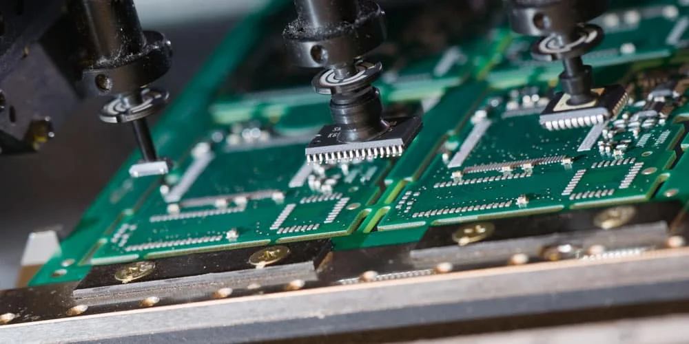
Pcb component placement directly influences the efficiency of high-volume batch assembly processes. In high-volume production, automated pick-and-place machines position components quickly and accurately. Poor placement strategies can lead to increased assembly time, higher defect rates, and challenges in testing or rework. For instance, components placed too close together may cause issues with machine access or soldering quality. Additionally, improper orientation can disrupt the flow of automated assembly lines, causing delays. Adhering to DFM for batch production ensures that designs are compatible with manufacturing equipment capabilities and minimizes manual intervention. Ultimately, optimizing pcb component placement through strategic placement reduces production bottlenecks, enhances yield, and ensures consistent quality across batches, which is critical for meeting project timelines and cost targets.
Understanding the technical aspects of pcb component placement is essential for achieving an efficient PCB design. The primary goal is to align the design with the capabilities of automated assembly systems while maintaining signal integrity and thermal performance. Key principles include alignment with pick-and-place machines (consistent orientation and minimum clearances to prevent collisions), grouping by functionality and size (e.g., clustering surface-mount resistors to reduce nozzle changes), consideration for signal integrity (short traces for high-speed signals and nearby decoupling capacitors), and thermal management (adequate spacing for power components and placement near heat sinks for optimal airflow).
Related Reading: Mastering SMT Component Placement for Optimal PCB Design
How Placement Accuracy Impacts Batch Production Costs
Accurate pcb component placement is a major cost driver in high-volume batch assembly. Even minor misalignments or suboptimal layouts trigger cascading expenses in rework, scrap, downtime, and yield loss. Poor placement can increase overall production costs by 10–30% through added labor, materials, and delayed shipments.
The table below illustrates key impacts with real-world examples:
| Placement Issue | Cost Impact | Example / Data Impact |
|---|---|---|
| Inconsistent orientation | 10–20% higher rework labor | Misplaced polarity markers require manual correction on 5–10% of boards |
| Insufficient spacing | Up to 25% increase in defects & scrap | Solder bridging in dense clusters wastes components and adds $0.50–$2.00 per board |
| Shadowing during reflow | 15% lower first-pass yield | Taller parts blocking smaller ones causes incomplete solder joints |
| Poor fiducial or test-point access | Extended testing time + 5–15% downtime | Probes cannot reach points, adding hours per batch and raising inspection costs |
| Non-optimized sequence/grouping | 20–30% slower throughput | Frequent tool changes on chip shooters inflate machine runtime and energy costs |
Implementing DFM for batch production early eliminates these issues, converting potential cost overruns into predictable savings and higher profitability in high-volume runs.
Best Practices for Component Placement in Batch Assembly
Implementing effective pcb component placement guidelines can significantly enhance the efficiency of high-volume batch assembly. Below are actionable strategies for optimizing board layout and reducing assembly time.
Standardize Component Orientation
Ensure all components of the same type share a consistent orientation. For example, align diodes and capacitors with their polarity markers in the same direction. This uniformity simplifies programming for pick-and-place machines and reduces the risk of placement errors. Refer to industry standards like IPC-7351B for guidance on land pattern design and orientation.
Related Reading: Pick and Place Programming: A Step by Step Guide for PCB Assembly
Maintain Adequate Spacing
Adhere to minimum spacing rules between components to accommodate assembly equipment and soldering processes. Tight clustering can lead to solder bridging or insufficient access for rework. Standards such as IPC-2221B provide detailed recommendations on clearances based on component types and board density.
Prioritize Placement Sequence
Place critical components first, such as connectors and large ICs, to define the board’s primary layout. Then position smaller passive components around them. This hierarchical approach ensures stability during assembly and minimizes interference while aiding board balance for automated handling.
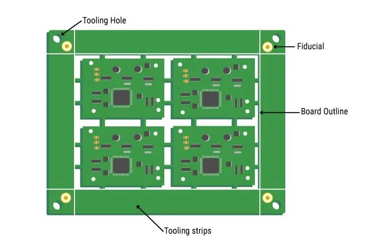
Optimize for Panelization
In high-volume batch assembly, multiple boards are produced on a single panel. Design pcb component placement to avoid interference with panel edges or breakaway tabs. Keep components away from areas designated for fiducial markers, which are essential for machine alignment.
Minimize Component Rotation
Limit rotation to 0° or 90° angles to align with standard machine capabilities. Non-standard angles increase programming complexity and slow down the assembly process, impacting overall efficiency.
Incorporate Test Points
Integrate test points in accessible locations to facilitate in-circuit testing after assembly. Position these points away from densely populated areas to ensure probes can reach them without obstruction. This practice supports quality control without necessitating design revisions.
Advanced Vision Systems
Modern SMT lines integrate advanced vision systems with high-resolution cameras and AI-driven algorithms for real-time component alignment and inspection. These systems detect offsets as small as 0.01 mm, automatically correcting placement before release and achieving accuracies of ±0.025 mm at speeds exceeding 100,000 components per hour. In high-volume batch assembly, vision-guided placement reduces misplacement rates by 80–90%, eliminates post-placement rework, and maintains throughput without sacrificing precision—critical for fine-pitch BGAs and 0201 components.
Chip Shooters for High-Speed SMT Efficiency and Precision
Chip shooters (turret-style high-speed mounters) excel in placing passive components at rates up to 200,000 CPH. Optimization involves intelligent feeder assignment and placement sequencing—grouping similar-sized parts to minimize turret rotation speed changes and using genetic algorithms or software to shorten head travel paths. Proper feeder layout and component size-based rotation control can improve overall line efficiency by 15–25%, directly boosting throughput in high-volume batch assembly while maintaining placement accuracy and reducing nozzle wear.
Account for Reflow and Wave Soldering
For reflow soldering, ensure smaller components are not shadowed by taller ones for even heat distribution. In wave soldering, place through-hole components on the bottom side with consistent orientation to match the wave direction, reducing defects like insufficient solder fill.
Addressing Common Challenges in Batch Assembly Placement
Even with careful planning, challenges can arise during high-volume batch assembly due to design oversights. One common issue is component misalignment caused by inconsistent silkscreen markings or fiducial inaccuracies. To mitigate this, ensure fiducials are placed in clear, unobstructed areas as per IPC-7351B guidelines. Another challenge is thermal imbalance during soldering, often due to uneven component distribution. Spread out heat-generating components and verify thermal profiles against standards like IPC-7530A for reflow processes. Additionally, high-density designs may lead to pick-and-place errors if spacing is inadequate. Review designs against IPC-2221B clearance rules to avoid such risks. Addressing these issues during the design phase prevents costly rework and ensures smooth production runs.
Conclusion
Effective pcb component placement is a cornerstone of successful high-volume batch assembly in PCB production. By adhering to well-established guidelines and prioritizing DFM for batch production, electrical engineers can create designs that optimize board layout and reduce assembly time. Consistent orientation, adequate spacing, strategic sequencing, and advanced tools like vision systems and optimized chip shooters are just a few practices that enhance manufacturing efficiency. Aligning designs with industry standards ensures compatibility with automated systems and minimizes production errors. As high-volume batch assembly demands precision and scalability, investing time in pcb component placement planning yields significant returns in cost savings and product reliability. These best practices empower engineers to bridge design and manufacturing, delivering high-quality PCBs that meet stringent performance criteria.
FAQs
Q1: What are the key component placement guidelines for high-volume batch assembly?
A1: Focus on consistency and accessibility. Orient components uniformly, maintain adequate spacing per IPC-2221B, and prioritize critical parts first. Group similar components to minimize tool changes. Ensure test points are accessible and avoid panel edge interference. These steps streamline production and support DFM for batch production.
Q2: How does optimizing pcb component placement reduce assembly time?
A2: Uniform orientation and logical grouping minimize machine reprogramming and tool swaps. Adequate spacing prevents errors, while strategic sequencing ensures smooth operation. Following DFM for batch production principles cuts manual adjustments and speeds up high-volume runs.
Q3: Why is DFM for batch production critical in PCB design?
A3: It ensures compatibility with automated processes, avoiding bottlenecks. By following standards like IPC-2221B, engineers prevent interference or soldering defects, lowering costs and improving yield in high-volume batch assembly.
Q4: What standards support efficient pcb component placement for high-volume batch assembly?
A4: IPC-7351B for land patterns and orientation, IPC-2221B for clearances, and IPC-7530A for thermal profiles. These ensure manufacturable designs that boost throughput and quality.
References
- IPC-7351B — Generic Requirements for Surface Mount Design and Land Pattern Standard. IPC, 2010.
- IPC-2221B — Generic Standard on Printed Board Design. IPC, 2012.
- IPC-7530A — Guidelines for Temperature Profiling for Mass Soldering Processes (Reflow & Wave). IPC, 2017.


