Introduction
Stencil aperture design forms the foundation of reliable solder paste deposition in the SMT assembly process. Engineers face constant challenges with defects like solder bridging, insufficient volume, and tombstoning, often tracing back to suboptimal aperture configurations. Mastering SMT stencil design requires a deep understanding of aperture size, shape, and their interaction with stencil thickness and paste rheology. This comprehensive guide draws on established engineering principles to equip electric engineers with practical strategies for high-yield production. By optimizing stencil aperture size and stencil aperture shape, assemblies achieve consistent solder joints that meet performance demands. Whether troubleshooting fine-pitch components or scaling high-volume runs, these insights deliver actionable results.
Understanding Stencil Apertures in SMT Stencil Design
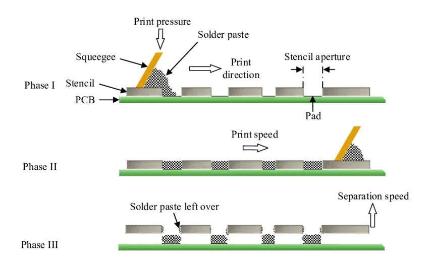
Stencil apertures are precisely cut openings in the metal foil that align with PCB pads during solder paste printing. They control the volume and placement of solder paste transferred to the board, directly influencing joint formation in subsequent reflow. Ineffective designs lead to variations in paste height, bridging between adjacent pads, or voids that compromise electrical reliability. Industry standards like IPC-7525B outline parameters to ensure repeatability across production. Aperture geometry must balance paste release from the stencil walls with sufficient deposit volume for robust joints. For electric engineers, recognizing these dynamics prevents costly rework and downtime.
The relevance of stencil aperture design extends to every stage of the SMT assembly process. Precise solder paste deposition minimizes defects, boosts first-pass yields, and supports miniaturization trends in electronics. Poor aperture control amplifies issues in high-density boards, where fine-pitch components demand tolerances below 50 microns. Engineers must consider paste particle size, stencil material, and printing parameters as interconnected factors. Optimizing these elements aligns with quality benchmarks, reducing inspection time and enhancing overall process capability. Ultimately, effective SMT stencil design translates to reliable assemblies under thermal and mechanical stress.
Key Technical Principles of Stencil Aperture Design
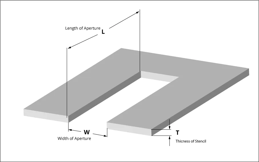
Stencil thickness typically ranges from 75 to 150 microns, dictating the baseline paste volume as aperture area multiplied by thickness. Aperture size should closely match pad dimensions, often at 90 to 100 percent for standard components to ensure coverage without excess. For fine-pitch leads below 0.5 mm, reducing aperture width by 10 to 20 percent prevents bridging while maintaining volume. Engineers calculate paste volume needs based on component type, targeting fillet heights per assembly standards. Deviations in stencil aperture size disrupt reflow behavior, leading to inconsistent joint profiles.
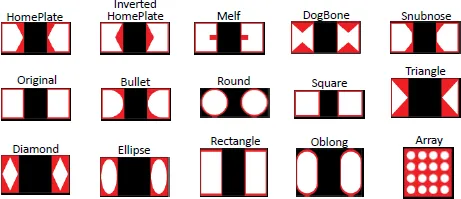
Stencil aperture shape profoundly impacts paste release and deposition uniformity. Rectangular apertures suit larger pads but struggle with release in narrow openings due to high wall contact area. Trapezoidal or U-shaped profiles reduce sidewall adhesion, improving clean lift-off during printing. Home-plate shapes work well for QFN peripherals, tapering to minimize paste smearing. The choice hinges on aspect ratio, defined as minimum aperture dimension divided by thickness, ideally exceeding 1.5 for reliable release. Area ratio, the open area to wall surface ratio, should surpass 0.66 to avoid insufficient transfer.
Paste rheology interacts with aperture geometry through the five-particle rule, where aperture width accommodates at least five times the largest paste particle diameter. Type 4 or finer pastes enable smaller apertures down to 0.2 mm without clogging. Thicker stencils demand wider apertures to maintain ratios, while thinner foils support ultra-fine pitch. Printing speed and pressure further modulate deposition, but aperture fundamentals set the limits. IPC-7525B emphasizes these ratios for consistent solder paste deposition across component densities.
Environmental factors like humidity affect paste viscosity, indirectly stressing aperture tolerances. Warped stencils or board bow exacerbate gasketing issues, causing skips or smears. Material selection, such as electroformed nickel for precision edges, enhances aperture fidelity over laser-cut alternatives in high-volume SMT. Engineers simulate volume transfer using software to predict reflow outcomes before fabrication. These principles ensure stencil aperture design supports defect-free transitions to pick-and-place and reflow.
Best Practices for Optimizing Stencil Aperture Size and Shape
Start with padstack analysis from design files to derive baseline aperture dimensions. Scale apertures to 100 percent pad area for pitches above 0.65 mm, reducing to 80 percent for 0.4 mm fine-pitch to control volume. Verify against component datasheets for peripheral array needs, like BGA underfill considerations. Stencil thickness selection drives the process: 125 microns for general use, 100 microns for miniatures, 150 microns for large passives. Always prototype prints to validate transfer efficiency above 75 percent.
Incorporate shape modifications for challenging features. Elongated D or scooped rectangles on gull-wing leads reduce bridging by 30 percent in trials. For via-in-pad, home apertures or teardrops channel paste away from vias. Maintain minimum 0.1 mm gaps between adjacent apertures to prevent merging during squeegee passes. IPC-7527 provides metrics for print process control, emphasizing aperture-to-pitch harmony. Regular stencil cleaning sustains edge sharpness, preserving design intent over thousands of cycles.

- Component Pitch > 0.65 mm — Aperture Scaling: 100% — Preferred Shape: Rectangular
- Component Pitch 0.5 mm — Aperture Scaling: 90% — Preferred Shape: Trapezoidal
- Component Pitch < 0.4 mm — Aperture Scaling: 75-80% — Preferred Shape: U-shaped or Home
Integrate process data from SPI for iterative refinement. Low volume prompts wider apertures or thinner stencils; bridging calls for narrower ones or scooped walls. Align squeegee angle at 60 degrees with 2-5 kg/cm2 pressure for optimal shear. These practices elevate SMT stencil design from art to science, troubleshooting root causes systematically.
Troubleshooting Common Stencil Aperture Issues
Insufficient solder paste deposition often stems from low area ratios below 0.66, causing poor release. Inspect apertures for burrs or rounding, which trap paste; nano-coatings mitigate this. Bridging in fine arrays traces to oversized stencil aperture size relative to pitch. Solution: Shrink by 5-10 percent and adopt type-5 paste for smoother flow. Tombstoning signals volume imbalance; balance apertures across chip ends.
Voids under BGAs indicate trapped air or uneven deposition. Use printed-and-plated vias or donut apertures to vent. Skips from gasketing failures require flatness checks per J-STD-001 criteria. Warped stencils demand fiducials and tensioning. Log defect Pareto charts to prioritize aperture tweaks, correlating SPI data with X-ray post-reflow.
Case insight: A high-density server board with 0.3 mm pitch saw 15 percent bridging. Switching to 75 percent scaled U-shapes with 100-micron thickness dropped it to under 1 percent yield gain. Such targeted adjustments resolve systemic issues efficiently.
Conclusion
Mastering stencil aperture design unlocks precision in the SMT assembly process, ensuring reliable solder paste deposition every time. Key to success lies in balancing size, shape, and ratios per industry guidelines like IPC-7525B. Electric engineers benefit from systematic approaches, from ratio calculations to troubleshooting protocols. Implementing these practices minimizes defects, accelerates yields, and supports advanced packaging. Prioritize simulation, prototyping, and data-driven iteration for sustained excellence.
FAQs
Q1: What is the optimal stencil aperture size for fine-pitch SMT components?
A1: For pitches below 0.5 mm, scale stencil aperture size to 75-90 percent of pad width to prevent bridging while ensuring adequate solder paste deposition. Maintain aspect ratio above 1.5 relative to stencil thickness. Verify with SPI measurements targeting 100-120 percent volume transfer. This approach aligns with SMT stencil design principles for reliable joints.
Q2: How does stencil aperture shape influence solder paste deposition?
A2: Shapes like trapezoidal or U reduce wall adhesion, improving release over rectangles in narrow apertures. They minimize smearing and enhance uniformity in the SMT assembly process. Select based on area ratio exceeding 0.66 for clean prints. Troubleshooting favors scooped profiles for high-density arrays.
Q3: What role do industry standards play in SMT stencil design?
A3: Standards like IPC-7525B define ratios and guidelines for aperture size and shape, ensuring consistency in solder paste deposition. They provide benchmarks for thickness, release criteria, and defect prevention. Adhering elevates process capability in production environments.
Q4: Common causes of bridging in stencil aperture design?
A4: Oversized apertures relative to pitch or poor paste release from low area ratios cause bridging. Fine-pitch components exacerbate this without shape optimization. Reduce size by 10 percent, adopt finer paste, and check gaps. Systematic SPI analysis resolves most cases quickly.
References
IPC-7525B — Stencil Design Guidelines. IPC, 2011
IPC-7527 — Requirements for Solder Paste Printing. IPC, 2007
J-STD-001H — Requirements for Soldered Electrical and Electronic Assemblies. IPC/JEDEC, 2018