Introduction
Pressure sensors play a vital role in modern electronics, enabling precise monitoring in applications ranging from automotive systems to medical devices and industrial automation. When integrating these sensors into printed circuit boards (PCBs), engineers must navigate a complex set of pressure sensor selection criteria to ensure optimal performance, reliability, and manufacturability. PCB design constraints such as limited space, thermal management, and mechanical stresses further complicate the process, demanding careful consideration of sensor specifications against board-level requirements. This comprehensive guide provides electric engineers with structured insights into key factors like pressure range requirements, signal conditioning options, and environmental factors in selection. By following a systematic sensor integration checklist and prioritizing PCB footprint optimization, designers can achieve robust integrations that withstand real-world operating conditions. Ultimately, informed decisions here prevent costly redesigns and enhance overall system efficiency.
Understanding Pressure Sensors for PCB Applications
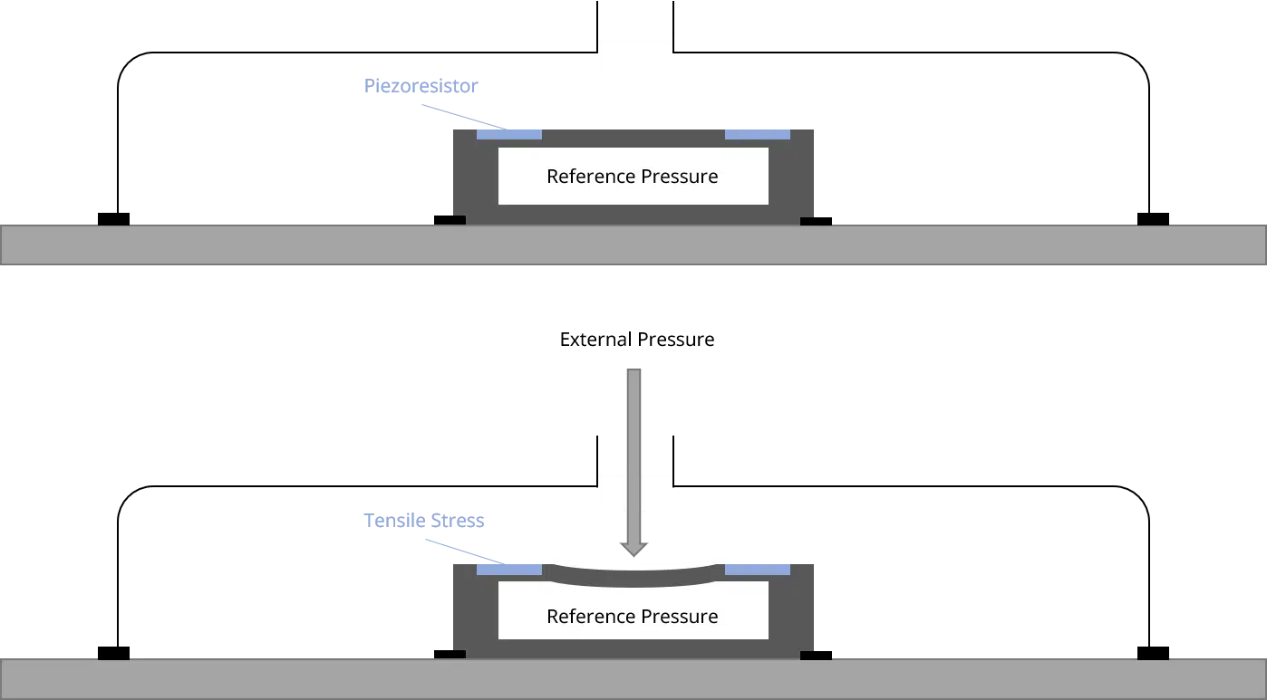
Pressure sensors detect and quantify force per unit area, converting mechanical pressure into electrical signals suitable for PCB processing. Common types include piezoresistive and capacitive sensors, each leveraging distinct transduction principles. Piezoresistive sensors employ strain gauges arranged in a Wheatstone bridge configuration, where applied pressure alters resistor values to produce a proportional voltage output. Capacitive sensors, in contrast, measure changes in capacitance caused by diaphragm deflection under pressure, offering advantages in temperature stability. These mechanisms directly influence suitability for PCB integration, as piezoresistive types excel in high-resolution applications but require compensation for thermal drift, while capacitive variants provide lower power consumption at the expense of higher sensitivity to electromagnetic interference. Selecting the appropriate type aligns sensor capabilities with PCB design constraints, ensuring signal integrity and long-term reliability.
The relevance of pressure sensors in PCB designs stems from their ubiquity in IoT devices, wearables, and control systems, where compact size and low power are paramount. Improper selection can lead to failures from mechanical stress or environmental exposure, underscoring the need for thorough evaluation. Engineers must weigh trade-offs in accuracy, response time, and hysteresis against application demands. For instance, differential sensors suit flow measurements, while absolute types fit barometric applications. This foundational understanding sets the stage for applying pressure sensor selection criteria effectively within PCB ecosystems.
Key Pressure Sensor Selection Criteria
Pressure sensor selection criteria begin with defining pressure range requirements, which dictate whether a gauge, absolute, or differential configuration is needed. Engineers must match the sensor's full-scale range to expected operating pressures, accounting for overpressure tolerance to prevent damage during transients. Accuracy specifications, including linearity, repeatability, and hysteresis, ensure measurement fidelity, typically expressed as a percentage of full scale. Response time and bandwidth are critical for dynamic applications like vibration monitoring, where fast settling prevents signal distortion. Output format—analog voltage, current, or digital interfaces like I2C or SPI—impacts PCB routing complexity and microcontroller compatibility. Power consumption rounds out core criteria, favoring low quiescent current for battery-operated designs.
Beyond basics, long-term stability and zero offset drift influence selection, particularly in precision environments. Cost-effectiveness must balance against performance, as higher accuracy often correlates with premium pricing. Media compatibility addresses corrosive fluids or gases, requiring diaphragm materials like silicon or ceramic. Mounting style—surface-mount device (SMD) versus through-hole—prioritizes PCB assembly processes. By systematically evaluating these pressure sensor selection criteria, engineers mitigate risks associated with mismatched specifications.
PCB Design Constraints in Sensor Integration
PCB design constraints impose significant limitations on pressure sensor choices, starting with spatial restrictions that demand compact footprints. Board thickness and flexure affect sensor performance, as mechanical stresses from warpage can induce offset errors in strain-based designs. Thermal considerations arise from sensor self-heating and reflow soldering peaks, necessitating devices with wide operating temperature ranges. Electrical noise from adjacent high-speed traces requires shielding and ground plane strategies during layout. Power supply noise sensitivity further constrains placement near voltage regulators. Addressing these PCB design constraints early through simulation tools ensures seamless integration.
Material selection for the PCB influences sensor longevity, with low-CTE laminates minimizing thermal mismatch. Via placement and trace widths must support sensor current demands without excessive resistance. Compliance with standards like IPC-2221 for generic printed board design aids in navigating these challenges. Vibration and shock transmission through the board demand sensors with robust packaging. Proactive management of these constraints transforms potential pitfalls into reliable design features.
Sensor Integration Checklist
A structured sensor integration checklist streamlines the process, beginning with verifying moisture sensitivity level (MSL) per IPC/JEDEC J-STD-020F to ensure reflow process compatibility. Confirm pressure range requirements align with application maxima and minima, including safety margins. Evaluate signal conditioning options for amplifying weak outputs and filtering noise. Assess PCB footprint optimization using standardized land patterns to prevent soldering defects. Check environmental factors in selection, such as operating temperature and ingress protection. Prototype testing validates mechanical mounting stability under expected loads.
Key checklist items include:
- Compatibility with assembly processes (SMD reflow, wave soldering).
- Electrical interface matching (voltage levels, pull-ups for digital).
- Calibration provisions post-integration.
- Documentation review for handling and storage guidelines.
- Simulation of thermal and stress profiles.
This sensor integration checklist reduces integration errors, fostering first-pass success in production.
PCB Footprint Optimization Strategies
PCB footprint optimization hinges on adhering to IPC-7351B guidelines for surface mount land patterns, which define pad dimensions, spacing, and tolerances for reliable soldering. Density levels—most, nominal, least—allow tailoring to fabrication capabilities, with nominal often suiting high-volume assembly. Sensor package types like QFN or LGA require courtyard definitions to prevent component overlap. Thermal pads for heat dissipation demand via stitching to inner planes. Courtyard and silkscreen markings enhance assembly accuracy. Optimization balances solder joint integrity with board real estate efficiency.
Finite element analysis predicts stress concentrations at footprint edges, guiding relief cuts or standoffs. Solder mask expansion prevents bridging while maintaining coverage. For pressure sensors, port alignment with pressure inlets necessitates precise fiducials. Iterative DFM reviews refine footprints pre-layout. Effective PCB footprint optimization minimizes defects and enhances yield.
Signal Conditioning Options for Pressure Sensors
Signal conditioning options transform raw sensor outputs into usable forms, starting with instrumentation amplifiers for millivolt-level piezoresistive signals. Low-noise op-amps provide gain while rejecting common-mode interference. Filtering circuits—low-pass RC or active—attenuate high-frequency noise from EMI. Voltage references stabilize excitation supplies, reducing drift. Digital options like sigma-delta ADCs integrate conditioning with conversion. Selection depends on output impedance and bandwidth needs.
For digital sensors, minimal conditioning suffices, but SPI/I2C buffers protect against bus capacitance. Excitation current sources suit ratiometric configurations. Layout places conditioning circuitry close to sensors for impedance matching. Power sequencing prevents latch-up during startup. Robust signal conditioning options ensure high-fidelity data transmission across the PCB.
Environmental Factors in Selection
Environmental factors in selection profoundly impact pressure sensor reliability, with temperature extremes demanding compensated designs to counter drift. Humidity exposure risks corrosion, favoring hermetic or conformal-coated packages. Vibration and shock testing per industry protocols verifies mechanical resilience. Chemical media compatibility guides material choices like stainless steel ports. Altitude variations affect absolute sensors due to barometric shifts. Operating life under cyclic loading predicts fatigue.
Sealing ratings like IP67 protect against dust and moisture ingress. Thermal cycling stresses joints, addressed by flexible adhesives. Radiation hardness suits aerospace PCBs. Comprehensive evaluation of environmental factors in selection aligns sensors with deployment scenarios. Compliance with handling standards mitigates field failures.
Best Practices and Standards Compliance
Best practices emphasize early supplier collaboration for datasheet validation against requirements. Finite element modeling simulates PCB-sensor interactions under load. Design for testability includes accessible calibration points. Qualification follows IPC-6012 for rigid board performance specs. Multi-stage prototyping iterates on footprint and conditioning. Documentation traces decisions to criteria.
Adopting IPC-2221 principles standardizes design rules. MSL handling per J-STD-020F prevents popcorning. Lifecycle testing accelerates reliability assessment. These practices elevate PCB integrations to production-ready levels.
Conclusion
Navigating pressure sensor selection for PCB integration requires balancing pressure sensor selection criteria, PCB design constraints, and a rigorous sensor integration checklist. Prioritizing pressure range requirements, PCB footprint optimization via IPC-7351B, and tailored signal conditioning options ensures performance. Addressing environmental factors in selection fortifies designs against real-world stresses. By referencing standards like J-STD-020F, engineers achieve compliant, reliable assemblies. This guide equips electric engineers to make informed choices, driving innovation in compact, high-performance electronics.
FAQs
Q1: What are the primary pressure sensor selection criteria for PCB applications?
A1: Key pressure sensor selection criteria include pressure range requirements, accuracy, response time, output type, and power consumption. Engineers must also consider PCB design constraints like footprint size and thermal compatibility. Matching these to application needs prevents integration issues and ensures signal integrity. Adhering to standards like IPC-7351B for land patterns optimizes outcomes.
Q2: How does PCB footprint optimization impact sensor integration?
A2: PCB footprint optimization follows IPC-7351B to define precise land patterns, reducing soldering defects and stress points. Proper courtyard and thermal pad designs enhance heat dissipation and assembly yield. This addresses PCB design constraints, accommodating compact sensors without compromising reliability. Iterative DFM checks refine layouts for high-volume production.
Q3: What signal conditioning options suit pressure sensors on PCBs?
A3: Signal conditioning options range from instrumentation amplifiers for analog outputs to integrated ADCs for digital interfaces. Low-noise filters mitigate EMI, while references stabilize supplies. Placement near sensors minimizes noise pickup. Selection aligns with sensor impedance and PCB routing, boosting overall system accuracy per integration checklists.
Q4: How do environmental factors influence pressure sensor selection?
A4: Environmental factors in selection encompass temperature range, humidity, vibration, and media compatibility. Sensors must withstand thermal cycling and shock without drift. IP-rated packages protect against ingress. Evaluating these against J-STD-020F handling ensures reflow survivability, tailoring choices to harsh PCB deployments for extended reliability.
References
IPC-7351B — Generic Requirements for Surface Mount Design and Land Pattern Standard. IPC, 2005
IPC/JEDEC J-STD-020F — Moisture/Reflow Sensitivity Classification of Nonhermetic Surface Mount Devices. JEDEC, 2022
IPC-2221F — Generic Standard on Printed Board Design. IPC, 2020
IPC-6012E — Qualification and Performance Specification for Rigid Printed Boards. IPC, 2017