Introduction
Stencil aperture optimization plays a pivotal role in surface mount technology assembly, particularly when handling fine-pitch components. These components, with closely spaced leads, demand precise solder paste deposition to form reliable joints without defects like bridging or insufficient volume. Poorly designed apertures can lead to inconsistent solder paste printing, resulting in assembly failures that increase rework costs and delay production. Engineers must focus on fine pitch stencil design principles to balance paste release and volume control. This article explores the technical aspects of stencil aperture optimization, offering practical guidance for achieving optimal solder paste volume on pads. By understanding these factors, teams can enhance yield rates and ensure robust electronic assemblies.

Fine pitch stencil design requires attention to aperture geometry, stencil thickness, and printing parameters. Component bridging often arises from excess paste bridging adjacent pads, while inadequate solder paste volume leads to weak joints. Optimizing these elements aligns with industry practices to support high-density boards. The following sections delve into definitions, principles, and actionable strategies tailored for electric engineers tackling real-world challenges.
What Are Stencil Apertures and Why Do They Matter for Fine-Pitch Components?
Stencil apertures are precisely cut openings in a thin metal foil that define the pattern for solder paste application onto PCB pads. In fine pitch stencil design, these apertures must accommodate lead pitches below 0.5 mm, ensuring accurate transfer of solder paste during printing. The design directly influences solder paste volume, which is critical for forming symmetrical joints post-reflow. Without proper optimization, variations in paste height or shape can compromise joint integrity.
The relevance intensifies with shrinking component sizes in modern electronics. Fine-pitch devices like QFNs and CSPs challenge traditional stencil designs due to reduced pad areas and tighter tolerances. Component bridging becomes prevalent if apertures release too much paste, while low solder paste volume risks open joints. Stencil aperture optimization mitigates these risks by promoting consistent deposition efficiency. Engineers benefit from structured approaches to predict and control paste behavior.
Adhering to guidelines in IPC-7525C helps standardize fine pitch stencil design across processes. This standard outlines parameters for aperture shapes and ratios suited to high-density assemblies. Practical implementation reduces variability in solder paste printing outcomes. Ultimately, mastering these elements supports scalable production for complex boards.
Technical Principles of Solder Paste Deposition
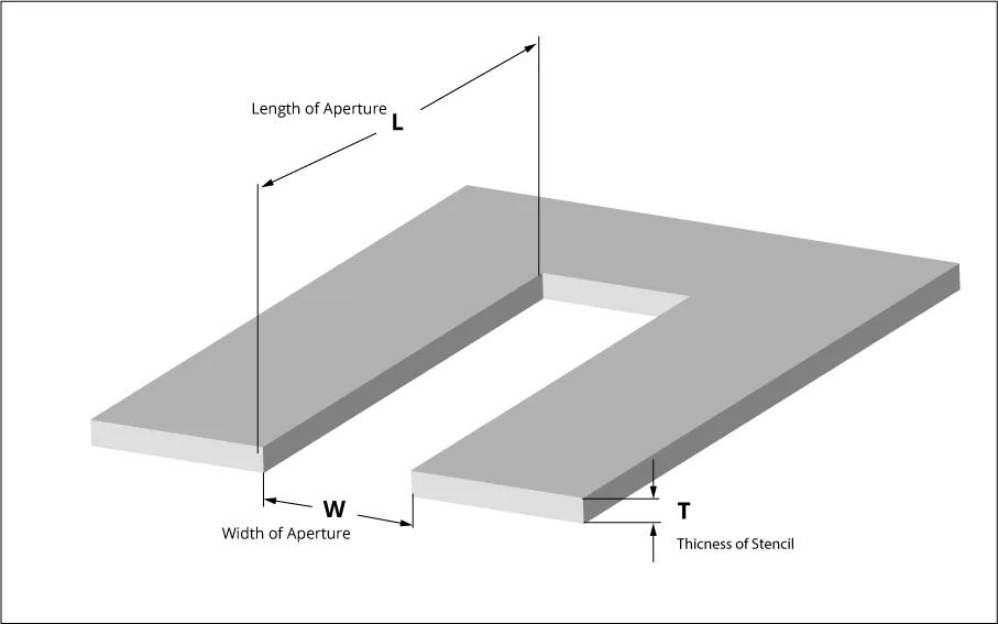
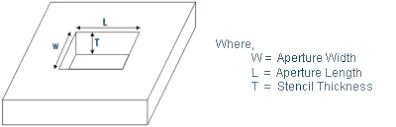
Solder paste deposition relies on the interaction between stencil apertures, paste rheology, and printing forces. During solder paste printing, the squeegee blade shears paste into apertures, followed by controlled release upon lift-off. Key factors include aspect ratio, defined as aperture width over thickness, and area ratio, which compares aperture open area to wall area. High area ratios facilitate better paste release, especially for fine-pitch features.
For fine-pitch components, stencil thickness typically ranges from 0.1 to 0.125 mm to maintain viable ratios. Thinner stencils improve release but may reduce solder paste volume for larger pads. Aperture walls must be smooth to minimize paste retention, as rough surfaces trap particles and cause defects. Engineers calculate ratios to predict transfer efficiency, aiming for consistent heights matching pad dimensions.
Paste composition affects deposition, with metal content and viscosity influencing flow into apertures. IPC-7525C provides guidelines on these ratios to ensure reliable solder paste printing. Understanding these principles allows proactive design adjustments. Variations in printing speed or pressure further modulate outcomes, requiring process validation.
Factors Influencing Stencil Aperture Performance
Several interrelated factors dictate stencil aperture performance in fine pitch applications. Aperture shape significantly impacts solder paste volume; rectangular openings often suffer from rounded corners post-print, reducing effective area. Trapezoidal or U-shaped apertures counteract this by promoting cleaner release and uniform height. Wall finish, achieved through electropolishing, reduces friction for better paste rollback.
Stencil material and fabrication method affect precision. Laser-cut stainless steel stencils offer tight tolerances essential for fine pitch stencil design. Frame tension and alignment during printing influence aperture-to-pad registration. Environmental controls, like humidity, prevent paste drying that clogs apertures.
Component bridging correlates with excessive paste bridging narrow gaps between pads. Low solder paste volume stems from poor transfer in high-aspect-ratio apertures. Optimizing these factors demands iterative testing. J-STD-005B specifies solder paste characteristics that interact with aperture design for optimal results.
Board warpage and pad finish also play roles, as uneven surfaces disrupt deposition. Engineers must integrate these considerations holistically. Data from print inspections guides refinements in stencil aperture optimization.
Best Practices for Stencil Aperture Optimization
Start with pad-to-aperture reduction, typically shrinking apertures by 5-10% relative to pads to control solder paste volume. This prevents paste overflow while ensuring adequate deposit for reflow. For fine-pitch leads, adopt home plating or scooped shapes to enhance release without volume loss. Maintain area ratios above recommended thresholds per IPC-7525C to support consistent printing.
Select stencil thickness based on the smallest pitch; 0.1 mm suits ultra-fine features, scaling up for mixed assemblies. Use software to simulate paste flow and validate designs pre-fabrication. Printing parameters like squeegee speed at 20-50 mm/s and pressure around 1-2 kg/cm promote even fill. Clean stencils between prints to avoid residue buildup affecting apertures.
Incorporate multi-level stencils for disparate pad sizes, thicker for larger pads to boost solder paste volume. Validate with SPI to measure height uniformity across apertures. Adjust based on feedback for ongoing stencil aperture optimization. These practices minimize defects in high-volume runs.
Troubleshooting Component Bridging and Solder Paste Volume Issues
Component bridging often traces to oversized apertures or high paste viscosity. Inspect prints for bridges narrower than pad gaps, indicating excess release. Reduce aperture width or switch to thinner stencils to curb volume. Slow squeegee speed allows better shear-off, breaking bridges effectively.
Insufficient solder paste volume appears as low-height deposits, leading to head-in-pillow defects post-reflow. Check area ratios; low values trap paste. Electropolish walls or refine shapes like adding corner reliefs. Verify paste age and storage, as stiffened paste prints poorly.
For persistent bridging in fine pitch stencil design, segment apertures or use type-4/5 pastes for finer particles. Analyze SPI data for patterns, correlating to specific aperture clusters. Process tweaks, like snap-off distance, fine-tune deposition. Systematic troubleshooting restores yield.
Warped boards exacerbate issues; ensure flatness before printing. Document changes in a DOE matrix for repeatability. These steps resolve common solder paste printing challenges efficiently.
Conclusion
Optimizing stencil apertures ensures precise solder paste deposition critical for fine-pitch components. Key principles like area ratios and shapes, guided by standards such as IPC-7525C, form the foundation. Practical best practices, from design reductions to process tuning, directly combat defects like component bridging and inconsistent solder paste volume. Troubleshooting with data-driven insights empowers engineers to refine fine pitch stencil design iteratively.
Implementing these strategies yields higher assembly success rates and reliable joints. Focus on validation at each stage to adapt to specific materials and components. Ultimately, stencil aperture optimization elevates overall SMT performance, supporting advanced electronics manufacturing.
FAQs
Q1: What role does area ratio play in fine pitch stencil design?
A1: Area ratio, the open aperture area divided by wall area, governs solder paste release during printing. Values above 0.66, as suggested in IPC-7525C, promote clean deposition for fine-pitch components. Low ratios cause retention, reducing solder paste volume and risking opens. Engineers calculate it early to select shapes like trapezoids, ensuring consistent heights and minimizing bridging.
Q2: How can engineers prevent component bridging in solder paste printing?
A2: Component bridging stems from excess paste between pads, often due to oversized apertures or fast printing speeds. Shrink apertures 5-10% from pad size and use smoother wall finishes via electropolishing. Opt for U-shaped designs in fine pitch stencil design to improve rollback. Validate with SPI and adjust squeegee pressure for optimal control.
Q3: Why is solder paste volume critical for fine-pitch components?
A3: Solder paste volume determines joint fillet formation post-reflow, vital for mechanical and electrical reliability. Inconsistent volume leads to voids or weak bonds in fine-pitch assemblies. Stencil aperture optimization via thickness selection and ratio adherence ensures targeted deposits. Monitor via height measurements to match IPC guidelines for robust performance.
Q4: What printing parameters affect stencil aperture optimization?
A4: Squeegee speed, pressure, and snap-off distance influence paste fill and release from apertures. Slower speeds aid fine pitch stencil design by reducing bridging, while moderate pressure ensures complete transfer. Humidity control prevents paste slumping. Tune these iteratively based on SPI feedback for uniform solder paste volume.
References
IPC-7525C — Stencil Design Guidelines. IPC, 2021
J-STD-005B — Requirements for Soldering Pastes. IPC, 2011