Introduction
Printed Circuit Boards (PCBs) form the backbone of modern electronics, enabling the functionality of devices across industries from consumer gadgets to aerospace systems. For electrical engineers, understanding the PCB manufacturing process is essential to ensure designs translate into reliable, high-quality products. This comprehensive guide walks through each stage of PCB fabrication, from initial design to final inspection, while aligning with globally recognized industry standards. Key aspects such as PCB etching, drilling, solder mask application, and surface finish selection are covered in detail. By grasping these steps, engineers can optimize designs for manufacturability and avoid common pitfalls during production. Whether you are refining a PCB stackup or troubleshooting fabrication issues, this article provides actionable insights to enhance your workflow.
What Is PCB Manufacturing and Why It Matters
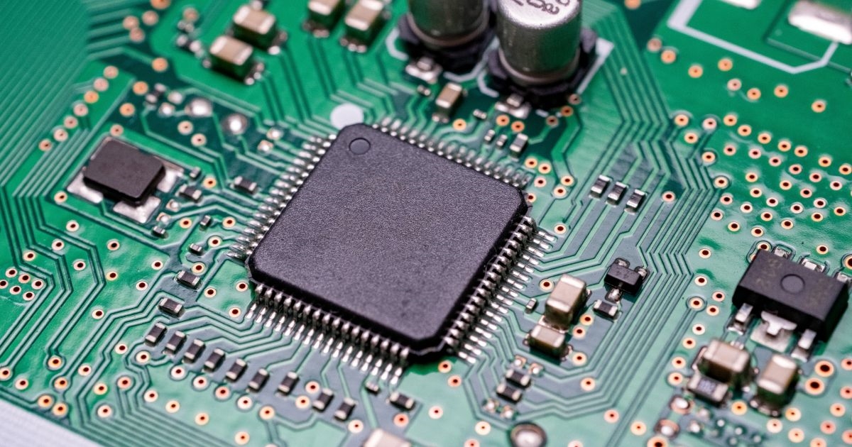
PCB manufacturing refers to the series of processes involved in creating a functional printed circuit board from a design blueprint. It encompasses PCB fabrication, which focuses on building the bare board, and PCB assembly, which involves mounting electronic components onto the board. This process is critical because the quality of a PCB directly impacts the performance, reliability, and lifespan of electronic devices. A poorly manufactured PCB can lead to signal integrity issues, thermal failures, or mechanical defects. For electrical engineers, a deep understanding of these steps ensures that designs are feasible for production and meet stringent requirements set by standards like those from IPC and ISO. Mastery of PCB manufacturing also aids in cost optimization and faster time to market.
Technical Principles of PCB Manufacturing
Design and Data Preparation
The PCB manufacturing journey begins with design data preparation. Engineers create detailed layouts using electronic design automation tools, defining the PCB stackup, trace widths, and component placements. This stage involves generating Gerber files, which are standardized formats for conveying design information to manufacturers. Accurate data preparation is crucial to avoid errors during subsequent fabrication steps. Compliance with standards such as IPC-2221B, which governs generic PCB design principles, ensures that designs are manufacturable and reliable.
Inner Layer Fabrication for Multilayer Boards
For multilayer PCBs, the process starts with inner layer fabrication. Copper-clad laminate sheets are coated with a photosensitive film, and the design pattern is transferred using ultraviolet light exposure. Unwanted copper is removed through PCB etching, leaving behind the desired conductive traces. This step demands precision to maintain trace integrity. Standards like IPC-6012E outline performance specifications for rigid PCBs, ensuring inner layers meet electrical and mechanical requirements.
Lamination and Stackup Formation
Once inner layers are prepared, they are stacked with insulating prepreg material and bonded under heat and pressure to form the PCB stackup. This lamination process creates a unified multilayer structure. Engineers must specify the correct dielectric materials and copper thicknesses to achieve desired electrical properties. Adhering to IPC-600K for acceptability criteria helps maintain structural integrity during this phase.
Related Reading: PCB Stack Up to Plan, Design, Manufacture and Repeat
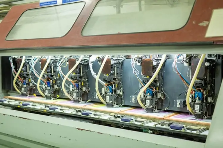
Drilling for Vias and Through-Holes
PCB drilling follows lamination, creating holes for vias and through-hole components. High-speed drills create precise openings, often down to fractions of a millimeter. These holes are later plated with copper to establish electrical connections between layers. Drilling accuracy is vital to prevent misalignment, and standards such as IPC-6012E provide guidelines for hole quality and tolerances.
Copper Plating and Outer Layer Processing
After drilling, the board undergoes copper plating to coat the drilled holes and reinforce outer layers. A thin layer of copper is deposited via an electroplating process, ensuring conductivity through vias. Outer layer imaging and etching then define the final circuit patterns. This step mirrors inner layer fabrication but focuses on external traces. Compliance with IPC-A-600K ensures that plating thickness and trace quality meet industry expectations.
Solder Mask Application
The solder mask is a protective layer applied to the PCB to prevent short circuits and oxidation. It covers copper traces while leaving component pads exposed for soldering. Typically, a green epoxy-based material is used, though other colors are available. The solder mask is applied using a screen-printing or photo-imaging process, then cured under heat. This layer also enhances the board’s durability. IPC-SM-840E provides qualification criteria for solder mask performance.
Silkscreen Printing
Silkscreen printing adds legible markings to the PCB, such as component identifiers and reference designators. This layer, often white, is applied over the solder mask using inkjet or screen-printing techniques. Clear and accurate silkscreen ensures ease of assembly and troubleshooting. While not critical to functionality, it aligns with IPC-A-600K standards for visual acceptability.
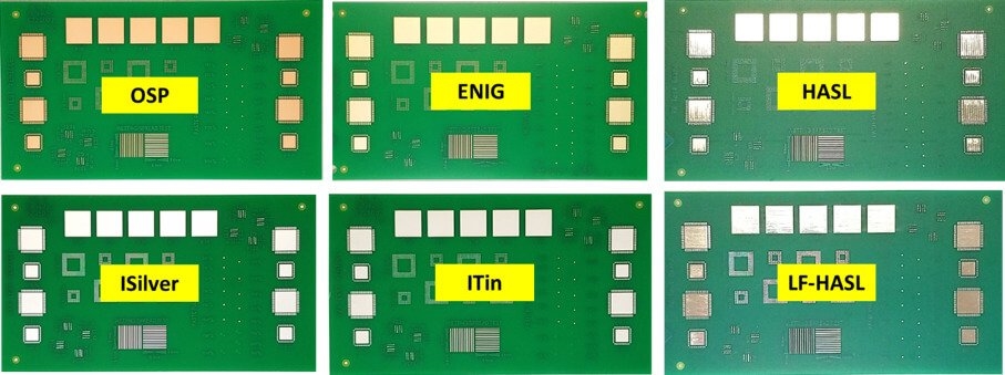
Surface Finish Selection
Surface finish is applied to exposed copper pads to prevent oxidation and enhance solderability. Common finishes include Hot Air Solder Leveling (HASL), Electroless Nickel Immersion Gold (ENIG), and Immersion Silver. Each finish offers distinct advantages, such as cost-effectiveness or superior corrosion resistance. Selection depends on application requirements and assembly processes. JEDEC J-STD-609A guides labeling and handling considerations for surface finishes.
Related Reading: Optimizing RF PCB Performance: The Crucial Role of Surface Finish Selection
Electrical Testing and Inspection
Before assembly, PCBs undergo electrical testing to verify connectivity and detect shorts or opens. Techniques like flying probe testing or bed-of-nails testing are employed. Visual and automated optical inspections check for defects in solder mask, silkscreen, or drilling. Adherence to IPC-A-600K ensures that boards meet acceptability criteria, minimizing risks during PCB assembly.
PCB Manufacturing Process Steps
Optimizing Design for Manufacturability
To streamline PCB fabrication, engineers should prioritize design for manufacturability (DFM). This involves adhering to minimum trace widths, spacing rules, and via sizes as outlined in IPC-2221B. Simplifying the PCB stackup reduces lamination complexity, while clear documentation prevents miscommunication with fabricators. Early collaboration during design can mitigate costly revisions.
Material Selection for Reliability
Choosing appropriate materials is fundamental to PCB performance. Base laminates, such as FR-4, must balance cost, thermal stability, and dielectric properties. Copper foil thickness impacts current-carrying capacity and etching precision. Engineers should consult standards like IPC-4101E for laminate specifications to ensure compatibility with intended applications.
Managing PCB Etching Precision
PCB etching requires careful control to avoid under-etching or over-etching, which can compromise trace integrity. Chemical solutions must be monitored for consistency, and process parameters adjusted based on copper thickness. Following guidelines from IPC-6012E helps achieve uniform etching results, critical for high-frequency or high-density designs.
Related Reading: The Art of Automotive PCB Etching: A Step by Step Guide
Streamlining PCB Assembly Processes
During PCB assembly, components are mounted using surface-mount technology (SMT) or through-hole methods. Solder paste is applied to pads, followed by component placement and reflow soldering. Engineers must ensure thermal profiles align with JEDEC J-STD-020E to prevent component damage. Automated inspection post-assembly verifies placement accuracy and solder joint quality.
Troubleshooting Common Manufacturing Issues
Addressing Drilling Misalignment
Drilling misalignment can disrupt via connectivity, leading to electrical failures. This often stems from improper machine calibration or material warpage. Engineers should specify tight tolerances in design files and verify fabricator capabilities. Post-drilling inspection per IPC-6012E standards helps identify and rectify issues early.
Correcting Solder Mask Defects
Solder mask defects, such as incomplete coverage or pinholes, expose copper to oxidation. This may result from uneven application or curing issues. Adjusting exposure parameters and ensuring cleanliness during application resolves most problems. Referencing IPC-SM-840E aids in defining acceptable defect levels.
Related Reading: Solder Mask Misalignment: Causes, Consequences, and Solutions for Robust PCB Production
Preventing Surface Finish Inconsistencies
Inconsistent surface finish can hinder solderability or cause reliability issues. Variations in plating thickness or contamination are common culprits. Strict process controls and adherence to JEDEC J-STD-609A during application ensure uniform finish quality across batches.
Conclusion
The PCB manufacturing process is a complex sequence of steps that transforms design concepts into functional boards. From initial data preparation to final surface finish application, each stage demands precision and adherence to industry standards like those from IPC and JEDEC. Electrical engineers who understand PCB fabrication, etching, drilling, and assembly can better optimize designs for reliability and cost efficiency. By focusing on material selection, process control, and thorough inspection, potential issues can be minimized. This guide serves as a foundation for navigating the intricacies of PCB production, ensuring high-quality outcomes for diverse applications.
FAQs
Q1: How does PCB etching impact the quality of a printed circuit board?
A1: PCB etching directly affects trace accuracy and electrical performance. If not controlled, over-etching can thin traces, increasing resistance, while under-etching may leave unwanted copper, risking shorts. Following standards like IPC-6012E ensures precise removal of excess copper. Proper chemical monitoring and process adjustments are essential for consistent results, especially in high-density designs.
Q2: What factors should engineers consider during PCB drilling?
A2: During PCB drilling, engineers must consider hole size, placement accuracy, and material properties. Misaligned or oversized holes can disrupt connectivity in vias or through-hole components. Specifying tolerances as per IPC-6012E and selecting appropriate drill speeds prevent defects. Material warpage should also be minimized to maintain precision across the board.
Q3: Why is solder mask application critical in PCB manufacturing?
A3: Solder mask application protects copper traces from oxidation and prevents short circuits during assembly. It ensures only designated pads are exposed for soldering, enhancing reliability. Defects like pinholes can compromise this protection. Adhering to IPC-SM-840E standards during application guarantees durability and performance under various environmental conditions.
Q4: How does surface finish selection influence PCB assembly outcomes?
A4: Surface finish selection impacts solderability and long-term reliability in PCB assembly. Finishes like ENIG offer excellent corrosion resistance, while HASL is cost-effective but less uniform. Choosing the right finish per JEDEC J-STD-609A ensures compatibility with soldering processes and environmental stresses. This decision affects both assembly quality and product lifespan.
References
IPC-2221B — Generic Standard on Printed Board Design. IPC, 2012.
IPC-6012E — Qualification and Performance Specification for Rigid Printed Boards. IPC, 2020.
IPC-A-600K — Acceptability of Printed Boards. IPC, 2020.
IPC-SM-840E — Qualification and Performance of Permanent Solder Mask and Flexible Cover Materials. IPC, 2011.
IPC-4101E — Specification for Base Materials for Rigid and Multilayer Printed Boards. IPC, 2017.
JEDEC J-STD-020E — Moisture/Reflow Sensitivity Classification for Nonhermetic Surface Mount Devices. JEDEC, 2014.
JEDEC J-STD-609A — Marking and Labeling of Components, PCBs and PCBAs to Identify Lead (Pb), Lead-Free (Pb-Free) and Other Attributes. JEDEC, 2011.


