Introduction
Electromagnetic Compatibility (EMC) remains a critical aspect of PCB prototyping assembly, ensuring that electronic devices function without interfering with other systems or being disrupted by external electromagnetic fields. For electric engineers, achieving EMC compliance is not just about meeting regulatory requirements but also about guaranteeing reliability and performance in complex environments. Issues like electromagnetic interference (EMI) can degrade signal integrity, cause system malfunctions, or lead to costly redesigns. This article explores the fundamentals of EMC in PCB design, focusing on practical strategies such as shielding techniques, filtering, grounding, and optimizing PCB layout for EMC. By understanding and applying these principles during the prototyping phase, engineers can reduce electromagnetic interference and build robust assemblies that meet stringent industry standards. Let’s delve into the technical aspects and actionable solutions for EMC optimization.
What Is Electromagnetic Compatibility (EMC) and Why It Matters
EMC refers to the ability of electronic equipment to operate in its intended environment without causing or experiencing electromagnetic interference. This concept is vital in PCB prototyping assembly because modern electronics often operate in close proximity to other devices, each emitting or susceptible to electromagnetic fields. Failure to address EMC can result in signal degradation, data errors, or complete system failure, especially in high-frequency or sensitive applications like medical, automotive, or aerospace systems.
Achieving EMC compliance involves two key components: emission control, which limits the electromagnetic energy a device radiates, and immunity, which ensures a device can withstand external interference. For electric engineers, prioritizing EMC during the prototyping stage minimizes the risk of non-compliance with international standards, avoiding delays and additional costs. It also enhances product reliability, a crucial factor in competitive markets where performance is non-negotiable.
Technical Principles of EMC in PCB Prototyping Assembly
Understanding the mechanisms behind electromagnetic interference is essential for effective PCB design. EMI can originate from conducted sources, where noise travels along power or signal lines, or radiated sources, where energy propagates through the air. In PCB assemblies, common causes include high-speed digital signals, switching power supplies, and improper grounding.
High-frequency signals on a PCB can create electromagnetic fields that couple with nearby traces, leading to crosstalk or unintended emissions. Similarly, switching components generate rapid voltage or current changes, producing noise that can interfere with sensitive circuits. Poor grounding practices exacerbate these issues by creating ground loops, where unwanted currents flow through multiple paths, amplifying interference.
Another key principle is the concept of impedance in signal paths. Mismatched impedance can cause signal reflections, increasing radiated emissions. Engineers must also consider the loop area formed by signal and return paths, as larger loops act as antennas, radiating more EMI. Addressing these factors during PCB layout for EMC is critical to minimizing interference at the source.

Practical Solutions for EMC Compliance in PCB Prototyping
Achieving EMC compliance requires a systematic approach during PCB prototyping assembly. Below are proven strategies focusing on shielding techniques, filtering, grounding, and layout optimization to reduce electromagnetic interference.
Shielding Techniques for EMI Reduction
Shielding involves enclosing sensitive components or entire PCB sections to block electromagnetic fields. Metallic enclosures or conductive coatings can contain radiated emissions from high-frequency circuits. For prototyping, engineers can use copper tape or temporary shields to test effectiveness before finalizing designs. Shielding must be connected to a low-impedance ground to prevent it from acting as an antenna. Additionally, compartmentalizing noisy and sensitive areas on the PCB with grounded metal barriers can isolate interference sources effectively.
Filtering to Suppress Noise
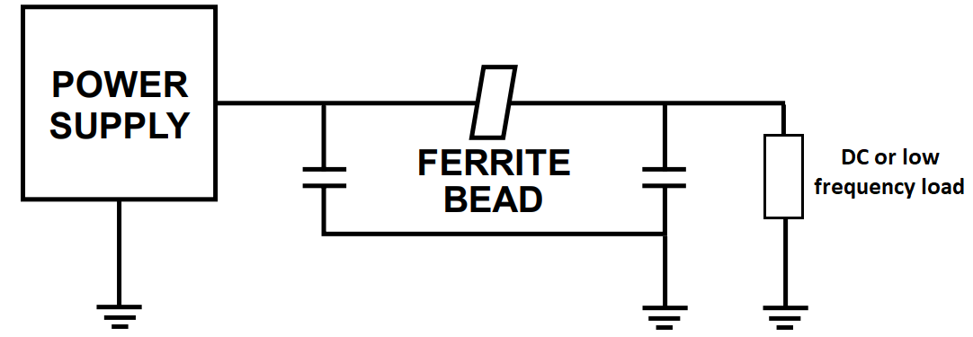
Filtering is a fundamental method to mitigate conducted EMI. Low-pass filters, comprising capacitors and inductors, can attenuate high-frequency noise on power lines. During prototyping, place filter components close to the power entry points of integrated circuits to block noise before it spreads. Ferrite beads paired with bypass capacitors are particularly useful for suppressing high-frequency noise in power supplies. Ensure that filter designs match the frequency range of expected interference for optimal performance.
Grounding Strategies for Stability
Effective grounding is the backbone of reducing electromagnetic interference. A solid ground plane minimizes impedance and provides a low-noise return path for signals. In multilayer PCBs, dedicate an entire layer to ground to reduce loop areas and enhance stability. Avoid splitting ground planes unless absolutely necessary, as splits can create high-impedance paths, leading to EMI issues. During prototyping, test different grounding configurations to identify the most effective setup for your specific application.
Related Reading: Improve Your Designs with the Best PCB Grounding Techniques
PCB Layout for EMC Optimization
Optimizing PCB layout for EMC starts with component placement and trace routing. Place high-speed components and noise sources away from sensitive analog circuits to minimize coupling. Keep signal traces short and direct, especially for high-frequency signals, to reduce loop areas. Route critical signals over a continuous ground plane to ensure a consistent return path. Additionally, maintain adequate spacing between traces to prevent crosstalk, adhering to guidelines provided by industry standards like IPC-2221B for general PCB design rules.
Decoupling Capacitors for Noise Reduction
Decoupling capacitors stabilize power supply voltages and absorb transient noise near active components. Place these capacitors as close as possible to the power pins of integrated circuits with short traces to minimize inductance. Use multiple capacitors with different values to cover a broad frequency range of noise suppression. This practice is especially critical in prototyping, where power integrity directly impacts EMC performance.
Related Reading: Designing a 6-Layer PCB for EMI/EMC Compliance: A Comprehensive Guide
Troubleshooting EMC Issues in Prototyping Assembly
During PCB prototyping assembly, EMC issues often surface during testing phases. Common problems include excessive radiated emissions or susceptibility to external interference. Engineers should use near-field probes to identify EMI hotspots on the board, focusing on areas with high-speed signals or switching components. Analyzing the frequency spectrum of emissions helps pinpoint specific noise sources, allowing targeted mitigation.
If grounding issues are suspected, verify the integrity of ground connections and check for unintended loops using continuity tests. For conducted EMI, review filter placement and component values, ensuring they align with the noise characteristics observed. Iteratively adjusting the PCB layout for EMC, such as repositioning components or rerouting traces, can resolve persistent issues. Documenting each test and modification ensures a clear path to achieving compliance in the final design.
Conclusion
Optimizing PCB prototyping assembly for Electromagnetic Compatibility is a multifaceted challenge that demands attention to detail and adherence to best practices. By focusing on shielding techniques, filtering, grounding, and strategic PCB layout for EMC, electric engineers can significantly reduce electromagnetic interference and achieve compliance with regulatory standards. These efforts during the prototyping phase lay the foundation for reliable, high-performance electronic products. Implementing the solutions outlined, from effective grounding to precise component placement, ensures that EMC issues are addressed early, saving time and resources in the development cycle. As electronics continue to evolve, prioritizing EMC remains essential for success in demanding applications.
FAQs
Q1: How does PCB layout for EMC impact overall design performance?
A1: A well-optimized PCB layout for EMC minimizes electromagnetic interference by reducing loop areas and ensuring proper signal return paths. It enhances signal integrity and prevents crosstalk between traces. Following industry guidelines, such as maintaining trace spacing and using ground planes, directly improves system reliability and helps achieve compliance with standards.
Q2: What are the most effective shielding techniques for reducing electromagnetic interference?
A2: Shielding techniques, such as using metallic enclosures or grounded conductive barriers, effectively block radiated EMI. Isolating noisy components from sensitive areas on the PCB also helps. Connecting shields to a low-impedance ground prevents them from becoming antennas, ensuring they contain interference during prototyping and final assembly.
Q3: Why is grounding critical for EMC compliance in PCB prototyping?
A3: Grounding provides a low-impedance path for return currents, reducing noise and preventing ground loops that amplify interference. A solid ground plane in PCB design stabilizes signals and minimizes EMI. Proper grounding practices are essential for meeting EMC compliance, as they directly influence the board’s immunity and emission characteristics.
Q4: How can filtering help in achieving EMC compliance during assembly?
A4: Filtering suppresses conducted noise on power and signal lines, a key factor for EMC compliance. Using low-pass filters or ferrite beads near power entry points of components blocks high-frequency interference. Correct filter selection and placement during prototyping ensure noise is managed effectively, supporting overall system performance.
References
IPC-2221B — Generic Standard on Printed Board Design. IPC, 2012.
IPC-6012E — Qualification and Performance Specification for Rigid Printed Boards. IPC, 2020.
IEC 61000-6-3:2020 — Electromagnetic Compatibility (EMC) - Part 6-3: Generic Standards - Emission Standard for Residential, Commercial and Light-Industrial Environments. IEC, 2020.
IEC 61000-6-1:2016 — Electromagnetic Compatibility (EMC) - Part 6-1: Generic Standards - Immunity for Residential, Commercial and Light-Industrial Environments. IEC, 2016.


