Introduction
Six-layer PCBs have become the standard platform for products that must pass Class B or Class A radiated and conducted emissions limits while maintaining signal integrity for multi-gigabit interfaces. The typical 6 layer PCB stackup (S1-GND-S2-PWR-S3-GND-S4) provides two solid reference planes and four routing layers, enabling robust 6-layer PCB EMC design guidelines to be implemented from the earliest schematic stage. Proper grounding techniques, shielding methods, filter placement, and return path management directly determine whether a design passes EMI/EMC pre-compliance testing on the first attempt.
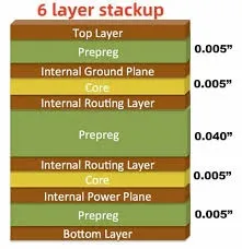
Recommended 6-Layer Stack-Ups for EMC
Preferred EMC Stack-Up (Foiled Construction)
- Layer 1: Signal (horizontal preferred)
- Layer 2: Solid Ground
- Layer 3: Signal (vertical preferred)
- Layer 4: Power (split as needed)
- Layer 5: Signal (horizontal preferred)
- Layer 6: Solid Ground
Key advantages:
- Every routing layer is tightly coupled to an adjacent solid reference plane
- Minimum 0.15–0.20 mm prepreg between signal and nearest plane
- Two dedicated ground planes enable low-inductance return paths
Alternative High-Performance Stack-Up
- Layer 1: Signal + GND fill
- Layer 2: Solid Ground
- Layer 3: Power (multiple rails)
- Layer 4: Power/GND (hybrid)
- Layer 5: Solid Ground
- Layer 6: Signal + GND fill
Used when additional power copper is required while preserving ground integrity.
Suggested Reading: 6-Layer PCB Stackup for Power Electronics: Design for High Current and Voltage
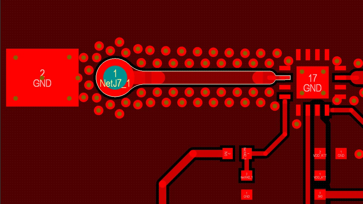
Core 6-Layer PCB Grounding Techniques
- Never split the primary ground planes (L2 and L5/L6). Keep them 100% solid with no cuts.
- Stitch ground planes together with via matrix every 10–15 mm along all board edges and under high-current areas.
- Connect all chassis or shield grounds directly to the nearest solid ground plane using multiple vias.
- Route high-speed return currents over the nearest unbroken plane. Avoid crossing plane gaps.
- Create local ground islands only for sensitive analog sections and bridge them with single-point connection or ferrite beads.
6-Layer PCB Shielding Methods
Internal Shielding
- Route sensitive traces on inner layers (L3 or L5) sandwiched between two ground planes
- Surround clock and high-speed differential pairs with ground vias every 5–8 mm (via fencing)
- Place guard rings tied to ground around crystal oscillators and RF sections
External Shielding Support
- Add continuous ground via fence 3–5 mm inside board edge for metal can attachment
- Provide dedicated chassis ground pads at all mounting holes
- Maintain 20-H rule: keep dielectric height to nearest plane less than 20 times trace-to-edge distance
Critical Filter and Component Placement Rules
Power Entry Filtering
- Place common-mode chokes and Y-capacitors as close as possible to connector entry
- Route DC power first to filter then to main power plane
- Keep filter input and output traces widely separated
Switching Regulator Layout
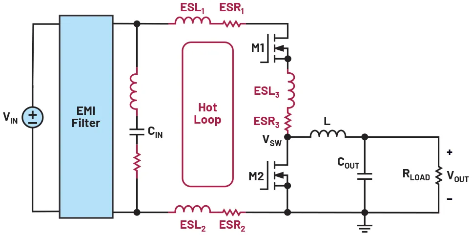
- Minimize hot loop area (MOSFET → inductor → output cap)
- Place input capacitors within 5 mm of VIN pin
- Route switching node on inner layer when possible
- Flood local ground copper directly under regulator IC
Clock and High-Speed Interface Routing
- Route clocks on inner layers adjacent to solid ground
- Avoid routing any trace parallel to clock for more than 10 mm
- Terminate unused clock outputs properly
- Keep differential pairs length-matched within 0.1 mm and spaced 2–3× width from other traces
Radiation Reduction Techniques
- 20 dB per decade rule: Every 10× reduction of loop area yields 20 dB lower radiation
- Spread spectrum clocking: Enable SSC on all high-frequency oscillators when permitted
- Slew-rate control: Use slower drivers for non-critical I/O to reduce harmonics
- Edge rate management: Keep rise/fall times above 1–2 ns for signals below 200 MHz
- Via fencing: Surround entire board and critical sections with ground vias spaced λ/20 or closer at highest frequency
Practical EMI/EMC Checklist for 6-Layer PCBs
- All routing layers adjacent to solid reference plane
- No signal crosses plane split at any frequency above 50 MHz
- Ground via spacing < 1/20 wavelength at highest frequency
- Common-mode filters at every cable interface
- Crystal and oscillator cases tied to ground with multiple vias
- I/O traces routed on inner layers when entering/exiting board
- Continuous ground pour on outer layers stitched every 10 mm
These practices complement proper high-speed PCB routing and impedance control strategies.
Conclusion
A well-executed 6 layer board with two solid ground planes and disciplined routing achieves Class B emissions margins of 6–10 dB on first-pass testing in most consumer and industrial products. The combination of tight layer-to-plane coupling, unbroken return paths, and strategic component placement forms the foundation of successful EMC design. Following these 6-layer PCB EMC design guidelines eliminates the majority of radiated and conducted emissions issues before the first prototype reaches the test chamber.
FAQs
Q1: Can I split a ground plane on a 6-layer PCB for analog/digital separation?
A1: Never split a solid reference plane. Instead, route analog signals on an inner layer over unbroken ground and use single-point connection or moat-and-bridge technique.
Q2: How close should ground stitching vias be placed?
A2: Maximum spacing should not exceed λ/20 at the highest frequency of concern or 10–12 mm in practice for systems up to 2 GHz.
Q3: Is it acceptable to route high-speed signals on outer layers of a 6-layer board?
A3: Only when absolutely necessary and with via fencing plus ground fill on the same layer. Inner layers sandwiched between planes always provide superior EMI performance.
Q4: Do I still need an external shield can with a proper 6-layer design?
A4: Many products pass Class B limits without metal shielding when the 6-layer PCB follows these guidelines, especially below 1 GHz. Shield cans become mandatory for 5G, Wi-Fi 6E, or automotive radar frequencies.
References
IPC-2221B — Generic Standard on Printed Board Design. IPC, 2015.
IPC-2152 — Standard for Determining Current Carrying Capacity in Printed Board Design. IPC, 2009.
IEC 61000-4-3 — Electromagnetic Compatibility (EMC) – Part 4-3: Radiated, Radio-Frequency, Electromagnetic Field Immunity Test. IEC, 2020.
CISPR 32 — Electromagnetic Compatibility of Multimedia Equipment – Emission Requirements. IEC, 2015.