Introduction
Power electronics push PCBs to handle surges in current and voltage. A 6-layer stackup offers robust layering for control signals and heavy power traces. In 6-layer PCB power electronics design, engineers focus on current paths that withstand 10A or more without overheating. This setup suits inverters and motor drives where reliability counts.
From assembly lines, I've seen boards fail under load due to thin coppers or poor isolation. High voltage demands careful spacing to prevent arcing. Optimizing stackups balances thermal dissipation with electrical safety. Key areas include copper thickness, heat management, and distance rules. This article shares practical tips from troubleshooting high-power builds. Learn to integrate 6-layer PCB copper weight for durability. Address 6-layer PCB thermal management for power to avoid hotspots. Ensure 6-layer PCB creepage and clearance meet safety needs. Enhance 6-layer PCB isolation for stable operation. These steps guide your designs toward field-proven performance.
6-Layer PCB Stackup for Power Electronics
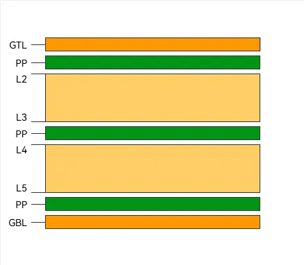
6-layer PCB stackup for power electronics involves arranging six conductive layers with dielectrics for high-current handling. It dedicates inner layers to power distribution and outer ones to signals. This structure supports voltages up to 600V in compact forms.
These stackups matter in demanding applications. Electric vehicles and renewable energy systems rely on them for efficient power conversion. Without proper layering, voltage drops erode efficiency. Assembly issues like delamination from thermal stress increase rework rates. In production, robust designs cut failures during high-current tests.
Experience shows 6-layer boards provide cost-effective scaling over simpler ones. They align with IPC-2221B for multilayer power routing. For safety, IPC-6012E qualifies boards under load. Procurement specifies these for projects needing thermal vias and thick coppers.
Technical Principles of 6 Layer Board Stackup in Power Electronics
Power design principles center on current density and dielectric strength. High currents generate I-squared-R losses, heating traces. Voltage gradients risk breakdown if insulation fails. Stackups mitigate these with balanced layering.
6-Layer PCB Copper Weight Considerations
Copper weight defines trace capacity in 6-layer PCB copper weight selection. Standard 1 oz per square foot handles 1A per mil width. Heavier 2 oz foils suit 20A paths without excessive width. IPC-2152 charts current-temperature rise limits.
Thicker coppers add rigidity but complicate etching. In multilayer PCB builds, inner layers use 2 oz for power while signals stay at 1 oz. Assembly notes uneven plating leads to shorts; uniform deposition ensures reliability.
6-Layer PCB Thermal Management for Power Basics
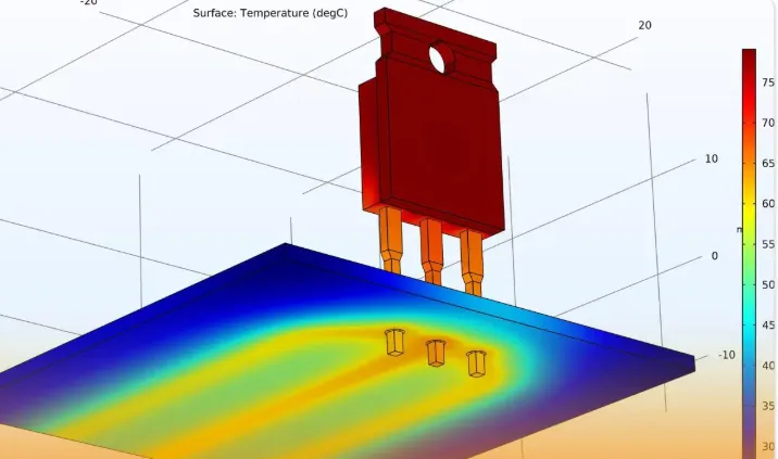
Thermal management in 6-layer PCB thermal management for power dissipates heat from components. Vias transfer warmth to inner planes acting as sinks. Dielectrics with high thermal conductivity, per IPC-4101E, spread loads evenly.
Junction temperatures must stay below 125°C for silicon devices. Poor flow causes hotspots, triggering thermal runaway. Layer sequencing places heat sources near outer edges for convection.
6-Layer PCB Creepage and Clearance Fundamentals
Creepage and clearance in 6-layer PCB creepage and clearance prevent surface and air breakdowns. Creepage measures along insulators; clearance through air. IPC-2221B tables pollution degrees and voltages, requiring 8 mm creepage at 500V.
High humidity amplifies risks, so conformal coatings add protection. In stackups, route high-voltage nets on dedicated layers to maximize distances.
Creepage, Clearance, and Isolation in 6 Layer PCB Stackup
Isolation in 6-layer PCB isolation separates power from low-voltage controls. Slots in planes block capacitive coupling. IPC-6012E demands 100 megohms minimum insulation resistance.
Guard rings around traces enhance separation. Experience reveals insufficient isolation sparks EMI during switching.
6 Layer PCB Stackup Design Guide for High Current and Voltage Applications
Build effective 6-layer power stackups with these steps. Plan layers as signal-ground-power-ground-power-signal. This sandwiches power between grounds for return paths.
For 6-layer PCB copper weight, specify 2 oz on power layers. Widen traces to 100 mils for 15A, per IPC-2152. Etch test patterns to verify yields.
Implement 6-layer PCB thermal management for power using filled vias under MOSFETs. Add copper pours connected to planes. Simulate with finite element tools for hotspot prediction.
Ensure 6-layer PCB creepage and clearance by routing HV on layer 3. Maintain 10 mm paths at 1000V. Use software autorouters with spacing rules.
Apply 6-layer PCB isolation with moats 0.5 mm wide around DC sections. Stitch grounds to planes every 10 mm.
Assembly practices include torque-controlled screws for heatsinks. Pre-bake boards to remove moisture per JEDEC J-STD-033D.
Troubleshooting Insights from Power Assembly Experience
Assembly floors expose stackup flaws under real loads. One build had a 6-layer inverter board with 5A hotspots. Cause: Undersized coppers on inner layers. Fix: Upped to 3 oz foils, dropping temps by 30°C after re-spin.
Voltage arcing plagued another design at 400V. Creepage paths contaminated during wave solder. Solution: Added slots and coatings, passing hi-pot tests at 1500V.
Isolation failures showed in control glitches. EMI coupled through unslotted planes. Routing HV away and adding ferrite beads resolved it.
Case from a motor drive: Thermal vias clogged with solder. Back-drilling cleared them, restoring flow. Yields jumped from 80% to 98%.
Suggested Reading: 6-Layer PCB Assembly Demystified: Best Practices for Reliable Manufacturing
Conclusion
6-layer PCB stackup for power electronics demands attention to copper, thermal, distance, and isolation details. These elements secure high-current and voltage handling. Practical tweaks from assembly ensure designs endure.
Follow IPC standards for validated outcomes. Test prototypes rigorously to catch issues. For your power projects, prioritize layered planning to deliver stable, efficient boards.
FAQs
Q1: How does 6-layer PCB copper weight affect power handling?
A1: 6-layer PCB copper weight boosts current capacity and lowers resistance. Thicker foils like 2 oz reduce voltage drops in high-amp paths. IPC-2152 guides sizing to limit 20°C rises. In assembly, heavier weights aid heat spreading but need precise etching.
Q2: What techniques improve 6-layer PCB thermal management for power?
A2: Improve 6-layer PCB thermal management for power with via stitching and plane pours. Place components over ground layers for conduction. Simulations predict flows before build. Experience shows embedded heatsinks cut junction temps effectively.
Q3: Why prioritize 6-layer PCB creepage and clearance in high-voltage designs?
A3: Prioritize 6-layer PCB creepage and clearance to avoid arcing in humid conditions. IPC-2221B sets minimums based on voltage classes. Coatings extend paths safely. Troubleshooting reveals contamination as a common failure mode.
Q4: How to enhance 6-layer PCB isolation in mixed-signal power boards?
A4: Enhance 6-layer PCB isolation with dedicated layers and ground moats. Stitch vias form barriers against coupling. IPC-6012E verifies resistance levels. Assembly tests confirm low EMI in operation.
IPC-2221B — Generic Standard on Printed Board Design. IPC, 2009.
IPC-6012E — Qualification and Performance Specification for Rigid Printed Boards. IPC, 2017.
IPC-2152 — Standard for Determining Current Carrying Capacity in Printed Board Design. IPC, 2009.
IPC-4101E — Specification for Base Materials for Rigid and Multilayer Printed Boards. IPC, 2010.
IPC-TM-650 — Test Methods Manual. IPC, various revisions.
JEDEC J-STD-033D — Handling, Packing, Shipping, and Use of Moisture/Reflow Sensitive Surface Mount Devices. JEDEC, 2018.


