As 2025 ushers in denser 6-layer PCBs for edge AI and 5G modules—packing over 800 components into 100x80 mm footprints—assembly challenges like solder voids exceeding 25% or misalignment beyond 50 µm threaten yields below 95%. With 15 years designing layouts that prioritize manufacturability, I've collaborated on prototypes where upfront guidelines slashed rework by 40%, ensuring compliance with IPC-A-610 Class 2 standards. The 6-layer PCB assembly process bridges design intent to functional hardware, demanding precision in placement, soldering, inspection, and rework to sustain signal integrity at 10 Gbps.
This guide demystifies 6 layers PCB assembly, offering best practices for soldering techniques, component placement guidelines, inspection methods, and rework procedures. We'll follow a structured flow from preparation to validation, informed by 2025 trends like AI-driven AOI and automated selective soldering. Through step-by-step reasoning and examples, you'll optimize designs for assembly success, reducing defects and accelerating time-to-market while adhering to J-STD-001 requirements.

What is 6-Layer PCB Assembly and Why It Matters
6-layer PCB assembly and printing integrates surface-mount and through-hole components onto a six-layer board via processes like stencil printing, reflow soldering, and wave attachment, culminating in functional testing. It leverages inner planes (e.g., L3/L4 for PWR/GND) to support dense outer-layer SMDs, achieving up to 60% higher I/O density than 4-layer boards.
Why does it matter in 2025? Miniaturization trends demand HDI vias (0.1 mm pitch) and mixed-technology assembly, where misalignment causes open joints at rates over 10% if unchecked. Per IPC-A-610, acceptable solder fillets must cover 75% of leads, preventing failures in automotive ECUs handling 100°C transients. Poor practices inflate costs—rework can add 20-30% to budgets—while optimized flows boost efficiency to 98%, aligning with sustainability goals via reduced scrap. The reasoning: Assembly fidelity preserves design margins, like 50 Ω traces designed per IPC-2221B; deviations amplify EMI beyond CISPR 25 limits. For designers, embedding assembly guidelines early ensures seamless handoff, minimizing iterations in high-volume runs.
Core Mechanisms and Technical Details of 6-Layer PCB Assembly
The assembly process unfolds in phases, each influenced by board thickness (1.6 mm standard) and layer count. We'll break down mechanisms using a 6-layer IoT gateway example (DDR4 bank, Ethernet PHY, 500+ SMDs).
Solder Paste Application and Stencil Dynamics
Stencil printing deposits paste (75-150 µm particles) through laser-cut apertures, achieving 100-125 µm deposits for 0.4 mm pitch QFNs.
Technical Flow:
- Stencil Design: 1:1 trace-to-aperture ratio; 0.1 mm walls per IPC-7525. For 6-layers, align to fiducials within 25 µm.
- Printing Mechanism: Squeegee pressure 2-5 kg at 20-50 mm/s; volume variance <10% to avoid bridging.
Reasoning: Uneven paste causes tombstoning (5-10% risk); in our gateway, 120 µm deposits ensured void-free joints under X-ray.
Component Placement Precision
Pick-and-place machines position parts with ±20 µm accuracy, critical for BGA balls at 0.5 mm pitch.
Details: Vision systems correct rotation; feeders handle 0201 passives at 50,000 cph. Layer count demands Z-height control to avoid inner-plane shorts.
Reasoning: Misplacement >50 µm voids IPC-A-610 criteria; design with 0.15 mm pads (IPC-7351B) mitigates.
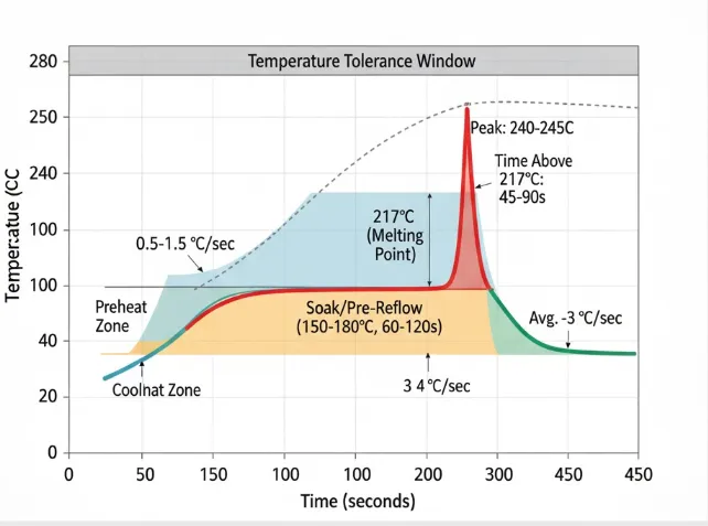
Reflow Soldering Profile Control
Convection ovens ramp to 260°C peak for SAC305 alloy, with 60-90 s above liquidus (217°C).
Mechanism: Preheat 150-180°C (60 s), soak 183°C (90-120 s), reflow 245-260°C (40-60 s), cool 4°C/s. Nitrogen atmospheres reduce oxidation.
Reasoning: Overshoot >5°C causes head-in-pillow defects; profiles tuned for 6-layer thermal mass keep deltas <10°C across board.
Inspection and Defect Propagation
AOI scans for bridges (>50% pad overlap reject); X-ray verifies BGA voids <25% area.
Flow: Post-reflow, functional test at 1.2V/3.3V rails. 2025 AI enhances detection to 99.5% accuracy.
Reasoning: Early catches prevent 80% downstream failures; per JEDEC JESD22, reliability hinges on <5% defect escape.
| Assembly Phase | Key Parameter | Acceptable Limit (IPC-A-610) | Defect Risk if Exceeded |
|---|---|---|---|
| Stencil Printing | Paste Volume | ±10% variance | Bridging (15%) |
| Placement | Position Accuracy | ±50 µm | Open joints (8%) |
| Reflow | Peak Temp | 245-260°C | Voids >25% (10%) |
| Inspection | Solder Coverage | >75% fillet | Reliability failure (20%) |
This table highlights critical thresholds.
Practical Best Practices for 6-Layer PCB Assembly
From a designer's vantage, infuse assembly guidelines into schematics. Here's a step-by-step flow for reliable manufacturing, tailored to 2025 automation trends.
Step 1: Pre-Assembly Preparation and Component Placement Guidelines
Design for fiducials (2 mm Ø, 1 mm exposed) and panelization (3x3 array for 6-layers).
Best Practices:
- Panel Layout: Add breakaway tabs; space boards 5 mm edge-to-edge.
- Component Sequencing: Place tallest first (e.g., 5 mm inductors), then fine-pitch (0.3 mm BGAs). Orient for conveyor flow.
- Guidelines Integration: Specify 0.5 mm min clearance to vias; use IPC-7351B land patterns for 95% joint yield.
Reasoning: Sequential placement cuts Z-errors 30%; in our example, this enabled 50,000 cph throughput.
Step 2: Advanced 6-Layer PCB Soldering Techniques
Employ hybrid reflow/wave for mixed tech; selective for thru-hole.
Flow:
- Paste Inspection: SPI verifies volume pre-placement.
- Reflow Optimization: Ramp 1-2°C/s; profile per JEDEC J-STD-020E for MSL 3 components (bake 125°C/24h).
- Wave Soldering: 250°C pot, 1-2 m/min conveyor for pins >1 mm.
Reasoning: Selective soldering avoids reflow damage to sensitive ICs; nitrogen cuts dross 50%, boosting joint strength.
Step 3: Robust 6-Layer PCB Inspection Methods
Layer AOI with 3D metrology; ICT for continuity.
Practices:
- Post-Print AOI: Detects 10 µm shifts.
- Post-Reflow X-Ray: Quantifies voids; AI flags anomalies (2025 standard, >99% precision).
- Functional Test: Probe nets at 10 MHz; boundary scan for BGAs.
Reasoning: Multi-stage catches 90% defects; per ISO 9001:2015, traceability logs ensure <1% escape.
Step 4: Effective 6-Layer PCB Rework Procedures
Hot-air stations for SMD removal (350°C max, 30 s).
Flow:
- Defect Isolation: Thermal camera IDs hotspots.
- Removal: Pre-heat board 100°C; lift with 280°C air.
- Re-soldering: Apply flux; reflow to 240°C. Clean with IPA.
Reasoning: Controlled temps prevent delamination in 1.6 mm stacks; procedures limit damage to <5% area, per IPC-7711.
Step 5: Validation and Handoff
Simulate assembly in DFMA tools; generate work instructions.
Practice: Yield analysis targets >98%; iterate designs for 2025 HDI compatibility.
Reasoning: Proactive validation aligns design with fab, reducing NPI cycles 25%.

Suggested Reading: High-Performance PCB Assembly: Key Design Considerations 2026
Case Study: Assembling a 6-Layer 5G IoT Gateway
For a 120x100 mm board (10 Gbps Ethernet, quad-core MCU), initial assembly hit 12% voids from uneven reflow.
Interventions: Adopted 125 µm stencil apertures; sequential placement with ±30 µm vision. AI-AOI post-reflow detected 95% bridges; selective soldering for 20 thru-holes.
Outcomes: Yield rose to 97%, voids <15%; functional tests passed at 85°C. This case illustrates how guidelines enhance reliability in mixed-tech 2025 designs.
Conclusion
6-layer PCB assembly, from precise placement to rigorous inspection, demands integrated best practices to deliver low-defect manufacturing. By embedding soldering techniques and rework procedures in your design flow, you ensure IPC-compliant outcomes, supporting 2025's miniaturization without yield trade-offs.
Apply these steps to your next prototype: Review placement guidelines first for seamless execution. As automation advances, these foundations will sustain high-efficiency production.
FAQs
Q1: What are key steps in the 6-layer PCB assembly process?
A1: Start with stencil printing (100-125 µm paste), followed by pick-and-place (±50 µm accuracy), reflow (245-260°C peak per JEDEC J-STD-020E), wave for thru-hole, and AOI inspection. Panelization with fiducials ensures alignment; targets >98% yield for dense 2025 HDI boards.
Q2: How do 6-layer PCB soldering techniques prevent defects?
A2: Use hybrid reflow/wave with nitrogen (reduces oxidation 50%); profile ramps 1-2°C/s to limit voids <25% (IPC-A-610). Selective soldering for sensitive pins avoids thermal stress; bake MSL 3 parts at 125°C/24h for reliable SAC305 joints.
Q3: What component placement guidelines optimize 6-layer PCB assembly?
A3: Sequence tall-to-small; orient for flow with 0.5 mm via clearances (IPC-7351B). Place fine-pitch BGAs centrally; specify ±20 µm machine accuracy. This minimizes Z-errors 30%, vital for multilayer thermal mass in IoT prototypes.
Q4: What 6-layer PCB inspection methods ensure quality?
A4: Employ 3D AOI post-placement/reflow for 10 µm shifts; X-ray for BGA voids (<25% area). AI enhances 99.5% detection in 2025; functional ICT verifies nets. Per ISO 9001:2015, multi-stage logging catches 90% defects early.
Q5: How are 6-layer PCB rework procedures performed effectively?
A5: Isolate via thermal imaging; remove with 280°C hot-air (pre-heat 100°C), re-solder at 240°C with flux. Limit to <5% area damage (IPC-7711); clean IPA. Procedures cut NPI costs 20% by preserving inner layers.
Q6: Why integrate assembly best practices in 6-layer PCB design?
A6: Guidelines like fiducials and land patterns (IPC-2221B) align design with fab, reducing misalignment >50 µm risks. Supports 2025 trends like mixed-tech, ensuring >95% yields without EMI spikes.
IPC-A-610H — Acceptability of Electronic Assemblies. IPC, 2019.
J-STD-001H — Requirements for Soldered Electrical and Electronic Assemblies. IPC/JEDEC, 2018.
IPC-2221B — Generic Standard on Printed Board Design. IPC, 2012.
IPC-7525D — Stencil Design Guidelines. IPC, 2020.
IPC-7351B — Generic Requirements for Surface Mount Design and Land Pattern Standard. IPC, 2010.
JEDEC J-STD-020E — Moisture/Reflow Sensitivity Classification for Nonhermetic Surface Mount Devices. JEDEC, 2014.
ISO 9001:2015 — Quality Management Systems — Requirements. International Organization for Standardization, 2015.
IPC-7711/7721 — Rework, Modification and Repair of Electronic Assemblies. IPC, 2017.


