Introduction
High-density PCB design demands compact layouts to accommodate increasing component counts and shrinking form factors. Engineers face challenges like limited routing space, via avoidance in multilayer boards, and maintaining signal integrity under tight constraints. SMD jumpers emerge as effective solutions by providing reliable, low-profile connections between traces without penetrating the board. These surface-mount devices function as zero-ohm links, enabling efficient bridging in areas where traditional through-hole jumpers or vias prove impractical. By integrating SMD jumpers, designers achieve higher component density while simplifying manufacturing processes. This approach aligns with the push toward miniaturized electronics in applications from consumer devices to telecommunications.
What Are SMD Jumpers and Why Do They Matter?
SMD jumpers are surface-mount components with nominal zero-ohm resistance, packaged in standard resistor formats like 0402, 0603, or 0805. They connect adjacent copper traces on the same layer, eliminating the need for vias or wire links in constrained areas. In high-density PCB design, these jumpers matter because they preserve valuable board real estate and support automated assembly lines. Unlike solder bridges, which risk shorts during rework, SMD jumpers offer precise, repeatable placements via pick-and-place machines. Their low profile, typically under 0.5mm height, allows traces to route beneath them on inner layers of multilayer boards. This capability proves essential for single-layer prototypes or cost-sensitive two-layer designs where vertical interconnects increase complexity.
The relevance extends to signal integrity, as SMD jumpers introduce minimal inductance and capacitance compared to longer wire jumps. Engineers select them for their compatibility with reflow soldering, ensuring uniform heating across the board. In evolving PCB trends, SMD jumpers facilitate faster time-to-market by reducing design iterations related to routing congestion.
Key Advantages of SMD Jumpers
SMD jumper advantages include significant space savings in high-density layouts, where every square millimeter counts. They enable routing optimization by bridging gaps without consuming via real estate, which can occupy up to 20% more area in dense boards. Machine-placeable nature streamlines surface-mount technology assembly, cutting labor costs and improving yield rates. Low parasitic effects make them suitable for high-frequency circuits, maintaining signal fidelity where inductors from wires might degrade performance.
Another benefit lies in design flexibility, allowing post-fabrication modifications by simply removing or replacing the jumper. This supports prototyping and field repairs without specialized tools. Compared to through-hole alternatives, SMD jumpers reduce board thickness and weight, critical for portable devices. Their integration also enhances thermal management in some variants, distributing heat more evenly across the PCB.

SMD Jumper Design Principles
SMD jumper design begins with selecting the appropriate package size based on current requirements and available pad space. Engineers must consider trace width compatibility to avoid bottlenecks in current flow paths. Proper orientation ensures the jumper aligns with the shortest path between pads, minimizing resistance and inductance. In multilayer boards, position jumpers to allow ground or power planes beneath for shielding.
Design tools generate footprints following established guidelines to ensure solder joint reliability. Factors like pad-to-pad spacing prevent bridging during reflow, while toe and heel fillet dimensions promote robust mechanical bonds. IPC-2221 provides foundational principles for such interconnect planning, emphasizing thermal and electrical performance. Balancing jumper size with board density avoids overpowering neighboring sensitive components.
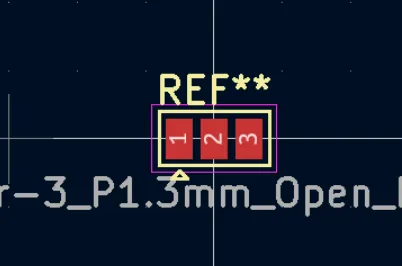
SMD Jumper Footprint Specifications
The SMD jumper footprint mirrors standard chip resistor land patterns, scaled to package dimensions for optimal solderability. Common sizes feature two rectangular pads separated by a gap matching the component's end terminations. Pad length typically exceeds termination width by 0.1 to 0.2mm for fillet formation, with width matching trace dimensions. IPC-7351 outlines nominal, reduced, and maximum density patterns, allowing customization for density levels.
Engineers verify footprint symmetry to prevent tombstoning during reflow, where uneven heating lifts one end. Solder mask clearance around pads, usually 0.1mm, isolates the jumper from adjacent features. For high-density PCB design, select footprints that permit trace fanout under the component on inner layers. Testing mockups confirms joint integrity under vibration and thermal cycling.
SMD Jumper Current and Voltage Ratings
SMD jumper current rating depends on package size, material, and termination construction, with smaller 0402 types handling around 0.5A and 0603 or 0805 reaching 1A to 2A continuously. Larger cross-sections in 0805 packages dissipate heat better, supporting higher currents without excessive temperature rise. Voltage rating follows SMD resistor norms, approximately 50V for 0402, 75V for 0603, and 150V for 0805, limited by dielectric strength across the body. Exceeding ratings risks arcing or melting, so derate by 50% in high ambient temperatures.
IPC-2152 guides current-carrying assessments, factoring trace width and copper thickness alongside jumper specs. Simulate thermal profiles to predict hotspot formation under load. Voltage standoff improves with wraparound terminations, common in robust designs. Always consult component datasheets for precise limits in the application context.
Thermal SMD Jumpers: Enhancing Heat Management
Thermal SMD jumpers differ from electrical types by prioritizing heat conduction over current carrying, using substrates like aluminum nitride for high thermal conductivity above 170 W/mK. Electrically isolated, they bridge hot components to PCB heatsinks or ground planes, lowering junction temperatures by efficient lateral heat spreading. Low thermal resistance, often under 1°C/W, suits power amplifiers and LEDs in dense layouts. Their SMD format integrates seamlessly with standard assembly flows.
In high-density PCB design, thermal SMD jumpers prevent hotspots by providing paths parallel to electrical traces. Pair them with via stitching for vertical heat escape. J-STD-001 criteria ensure solder joints withstand thermal stress without cracking. These jumpers prove vital where airflow is restricted, maintaining reliability in enclosed systems.
Best Practices for SMD Jumpers in High-Density PCB Design
Adopt IPC-7351 footprints to standardize land patterns across designs, ensuring consistency and manufacturability. Place jumpers early in layout to resolve routing blocks, prioritizing critical nets like power distribution. Maintain at least 0.15mm clearance to adjacent pads, reducing reflow bridging risks. Orient jumpers parallel to traces for minimal loop area, aiding EMI control.
Support jumpers with fiducials for precise placement, and specify no-clean flux for clean joints. In assembly, follow J-STD-001 for fillet inspection, verifying 75% heel coverage. For high-current paths, widen pads and use multiple jumpers in parallel. Simulate parasitics to confirm high-speed performance, adjusting if impedance mismatches arise. Document jumper locations in schematics as zero-ohm links for clarity.
Validate prototypes with X-ray for hidden defects and thermal imaging for hotspots. Iterate based on fab feedback, refining mask apertures for consistent paste volume.
Conclusion
SMD jumpers deliver space-saving solutions critical for high-density PCB designs, offering advantages in routing flexibility, assembly efficiency, and thermal management. From standard zero-ohm links to specialized thermal variants, they address key challenges in miniaturization without compromising performance. Proper SMD jumper design, footprint adherence, and rating considerations ensure reliability under operational stresses. Best practices grounded in industry standards maximize their benefits, enabling engineers to push density limits confidently. Integrating these components streamlines workflows from prototype to production, supporting innovative electronics.
FAQs
Q1: What are the main SMD jumper advantages in high-density PCB design?
A1: SMD jumper advantages include minimal footprint for space savings, compatibility with automated assembly, and low parasitics for signal integrity. They eliminate vias, reducing layer count and costs in multilayer boards. Placement allows traces underneath, optimizing routing in congested areas. Overall, they enhance manufacturability and design flexibility for electric engineers.
Q2: How do you select an SMD jumper footprint?
A2: Choose SMD jumper footprint based on package size matching current needs and pad availability, following IPC-7351 guidelines for density levels. Ensure pad dimensions form reliable fillets, with solder mask relief preventing shorts. Verify symmetry to avoid reflow defects like tombstoning. Test in prototypes for joint strength under thermal cycling.
Q3: What is the typical SMD jumper current rating?
A3: SMD jumper current rating varies by size, with 0402 around 0.5A, 0603 up to 1A, and 0805 reaching 2A continuously. Factor in derating for ambient heat and trace integration per IPC-2152. Voltage ratings scale similarly, 50V to 150V. Always simulate thermal rise for safety margins.
Q4: When should you use a thermal SMD jumper?
A4: Use thermal SMD jumper when electrical isolation with high heat transfer is needed, such as linking ICs to PCB heatsinks in power-dense boards. Their AlN substrate offers low thermal resistance for hotspot mitigation. Ideal for high-density designs with limited airflow. Ensure assembly per J-STD-001 for enduring bonds.
References
IPC-7351B — Generic Requirements for Surface Mount Design and Land Pattern Standard. IPC, 2005
IPC-2221B — Generic Standard on Printed Board Design. IPC, 1998
J-STD-001G — Requirements for Soldered Electrical and Electronic Assemblies. IPC, 2011