Introduction
Solder joints form the critical electrical and mechanical connections in printed circuit board assemblies (PCBA), directly impacting overall system performance and longevity. In demanding applications, these joints face thermal, mechanical, and environmental stresses that can lead to fatigue and failure. Engineers must prioritize solder joint reliability to minimize field returns and ensure compliance with quality expectations. This article explores PCBA solder joint fatigue mechanisms, established testing methods aligned with PCBA solder joint testing standards, failure analysis techniques, and proven strategies for PCBA solder joint reliability improvement. By understanding these elements, electric engineers can troubleshoot issues proactively and design more robust assemblies. Practical insights drawn from industry practices will guide implementation in real-world scenarios.
Understanding Solder Joints in PCBA and Their Importance
Solder joints in PCBA connect components to pads on the board, creating both conductive paths and structural bonds. These joints, typically formed during reflow soldering in surface-mount technology (SMT) processes, consist of solder alloy that wets the pad and lead surfaces. Reliability becomes paramount in environments with vibration, temperature fluctuations, or high power densities, where joints endure cyclic loading. Poor joint integrity can cause intermittent connectivity, signal loss, or complete circuit failure, leading to costly rework or product recalls. For electric engineers, assessing solder joint quality early prevents downstream issues in high-volume production. Focusing on joint microstructure and formation ensures assemblies withstand operational stresses over extended periods.
Mechanisms of PCBA Solder Joint Fatigue and Failure
PCBA solder joint fatigue primarily arises from repeated thermal expansion mismatches between the PCB substrate, components, and solder material. During operation, heating and cooling cycles induce shear stresses at the joint interfaces, promoting crack initiation and propagation. Mechanical vibrations or shocks exacerbate this by adding dynamic loads, accelerating fatigue in high-strain regions like corner components. Common failure modes include intermetallic compound growth, which embrittles the joint over time, and void formation from flux residues or improper reflow profiles. In lead-free solders, higher melting points amplify these effects under thermal cycling. Engineers troubleshooting fatigue must correlate field data with accelerated testing to identify dominant mechanisms in specific applications.
Other contributors to solder joint failure involve process-related defects such as insufficient solder volume, bridging, or tombstoning during assembly. Oxidation on pads or leads reduces wettability, resulting in weak bonds prone to early cracking. Humidity and contamination introduce electrochemical migration, further degrading joint strength. Understanding these mechanisms allows targeted interventions before failures escalate. By mapping stress distributions through finite element analysis, teams can predict vulnerable areas and adjust designs accordingly.
Related Reading: Ensuring PCB Reliability: A Deep Dive into Solder Joint Voids
PCBA Solder Joint Testing Standards and Methods
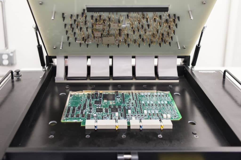
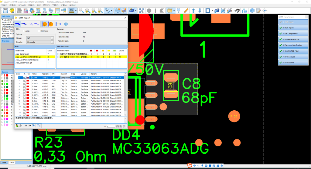
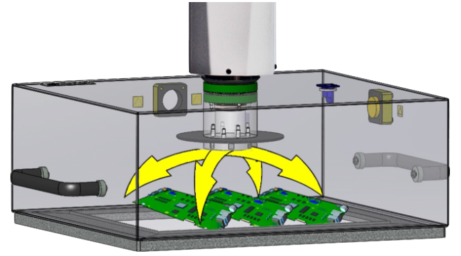
Testing solder joint reliability follows standardized protocols to simulate real-world conditions and quantify endurance. Thermal cycling tests, as outlined in IPC-9701, expose assemblies to controlled temperature swings to measure cycles-to-failure for surface-mount attachments. This method reveals fatigue life by monitoring electrical resistance changes indicative of cracking. Mechanical shock and vibration tests per IPC/JEDEC-9703 evaluate joint robustness under impact loads, using accelerometers to detect failures in drop-prone devices. These PCBA solder joint testing standards provide consistent benchmarks for qualification and process validation.
Additional methods include bend testing for flexible boards and four-point bend for evaluating warpage effects on joints. Electrical testing via daisy-chain monitoring tracks resistance spikes across multiple joints simultaneously. Acoustic microscopy detects voids non-destructively, while shear and pull tests assess mechanical strength post-assembly. Engineers select combinations based on end-use profiles, such as automotive versus consumer electronics. Integrating these tests into design verification ensures compliance and early defect detection.
PCBA Solder Joint Failure Analysis Techniques
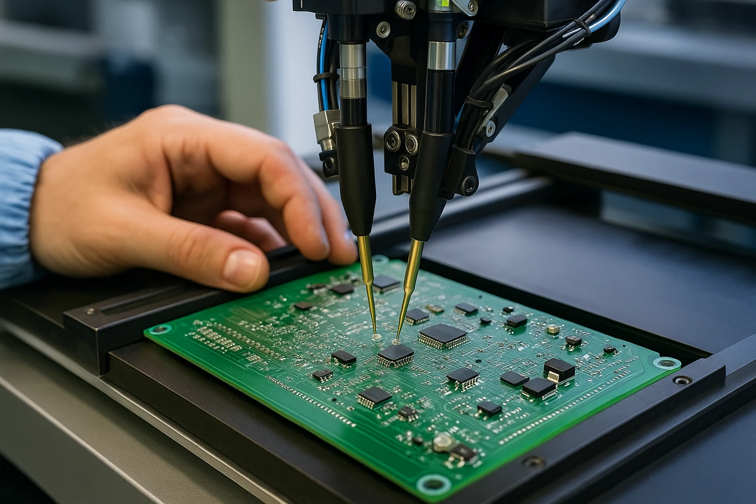
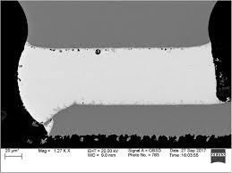
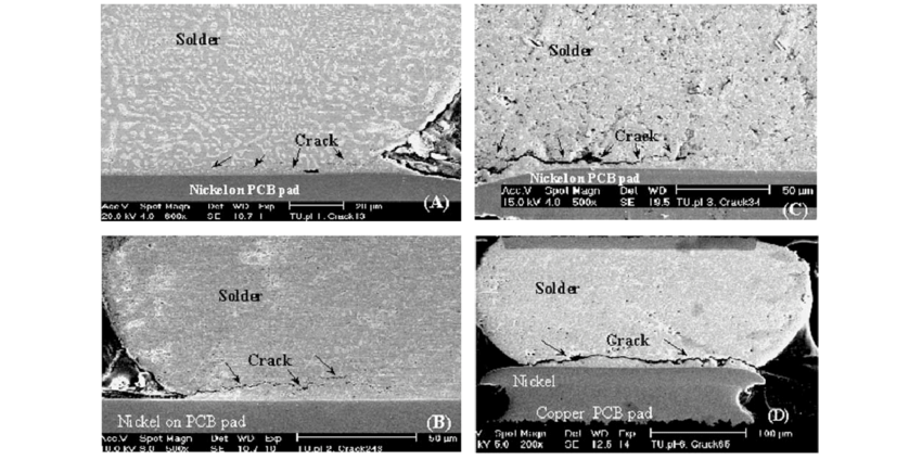
When failures occur, systematic PCBA solder joint failure analysis uncovers root causes through layered inspection techniques. Start with visual and optical microscopy to identify cracks, voids, or discoloration on joint surfaces. X-ray imaging reveals subsurface defects like head-in-pillow or bridging without disassembly. For deeper insights, cross-sectioning followed by scanning electron microscopy (SEM) examines microstructure, intermetallics, and fracture surfaces. Energy-dispersive X-ray spectroscopy (EDS) maps elemental composition to detect contamination or alloy issues.
Dye-and-penetrant testing highlights microcracks in inaccessible areas, while thermal analysis reconstructs reflow profiles from joint characteristics. Reliability engineers combine these with Weibull analysis of failure data to model distributions and predict field performance. Troubleshooting often points to upstream issues like stencil misalignment or paste printing defects. Documenting findings in failure modes and effects analysis (FMEA) prevents recurrence across production runs.
Related Readinig: Soldering Troubleshooting: Diagnosing and Fixing Common Solder Joint Issues
Best Practices for PCBA Solder Joint Reliability Improvement
Optimizing PCBA solder joint reliability improvement starts with precise reflow profiling to achieve uniform heating and minimize defects. Select solder pastes with compatible alloys and flux systems that promote wetting without excessive voids. Pad design per land pattern standards ensures adequate solder volume and fillet formation, reducing stress concentrations. Component standoff and orientation minimize warpage-induced strains during assembly.
Implement process controls like automated optical inspection (AOI) post-reflow to catch early anomalies. For high-reliability applications, precondition boards per J-STD-020 to simulate baking and reflow stresses. Vibration damping materials or underfill for ball grid arrays enhance mechanical integrity. Regular equipment maintenance prevents nozzle clogs or temperature drifts affecting paste deposition. Engineers should validate improvements through accelerated life testing, iterating on designs for extended mean time between failures (MTBF).
Material selection plays a key role, favoring low-CTE substrates matched to component packages. Finite element modeling simulates joint stresses pre-prototype, guiding layout adjustments. Collaborative reviews between design and assembly teams align expectations on tolerances and margins.
Conclusion
Solder joint reliability remains a cornerstone of PCBA durability, demanding vigilance across design, assembly, and testing phases. By mastering PCBA solder joint fatigue mechanisms, leveraging PCBA solder joint testing standards like IPC-9701 and IPC/JEDEC-9703, and applying rigorous failure analysis, engineers can achieve robust assemblies. Best practices in process control and material choices drive consistent PCBA solder joint reliability improvement, reducing risks in demanding environments. Proactive troubleshooting not only resolves issues but elevates overall product quality. Implementing these strategies ensures long-term performance and customer satisfaction in competitive markets.
FAQs
Q1: What are the primary causes of PCBA solder joint fatigue?
A1: PCBA solder joint fatigue stems from thermal cycling due to coefficient of thermal expansion mismatches, mechanical vibrations, and shock loads. Repeated stresses initiate microcracks that propagate over time, especially at joint heels and toes. Process defects like voids accelerate this under operation. Troubleshooting involves correlating test data with field failures to pinpoint dominant factors.
Q2: Which PCBA solder joint testing standards should engineers follow?
A2: Key PCBA solder joint testing standards include IPC-9701 for thermal cycling and IPC/JEDEC-9703 for mechanical shock. These provide protocols for qualifying surface-mount attachments under accelerated conditions. Compliance ensures predictable reliability across production lots. Select tests matching application profiles for accurate predictions.
Q3: How can PCBA solder joint reliability improvement be achieved in assembly?
A3: PCBA solder joint reliability improvement relies on optimized reflow profiles, precise stencil printing, and pad geometry adherence. Preconditioning per J-STD-020 mitigates moisture effects. AOI and X-ray verification catch defects early. Iterative testing refines processes for high-volume reliability.
Q4: What techniques are used in PCBA solder joint failure analysis?
A4: PCBA solder joint failure analysis employs X-ray for voids, SEM for microstructure, and resistance monitoring for cracks. Cross-sectioning reveals intermetallic growth, while EDS identifies contaminants. Layered approaches from non-destructive to destructive isolate causes efficiently.
References
IPC-9701 — Performance Test Methods and Qualification Requirements for Surface Mount Solder Attachments. IPC
IPC/JEDEC-9703 — Mechanical Shock Test Guidelines for Solder Joint Reliability. IPC/JEDEC
J-STD-001 — Requirements for Soldered Electrical and Electronic Assemblies. IPC/JEDEC
J-STD-020 — Moisture/Reflow Sensitivity Classification for Nonhermetic Surface Mount Devices. JEDEC